14 www.xilinx.com SP605 Hardware User Guide
UG526 (v1.1.1) February 1, 2010
Chapter 1: SP605 Evaluation Board
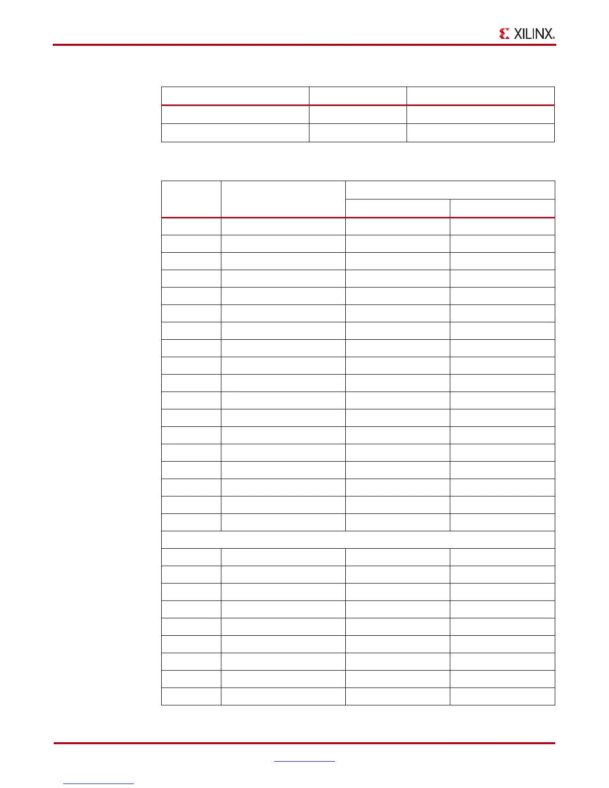
Table 1-5 shows the connections and pin numbers for the DDR3 Component Memory.
Table 1-4: FPGA On-Chip (OCT) Termination External Resistor Requirements
U1 FPGA Pin FPGA Pin Number Board Connection for OCT
ZIO P3 No Connect
RZQ L6 100 ohms to GROUND
Table 1-5: DDR3 Component Memory Connections
U1 FPGA
Pin
Schematic Net Name
Memory U42
Pin Number Pin Name
K2 MEM1_A0 N3 A0
K1 MEM1_A1 P7 A1
K5 MEM1_A2 P3 A2
M6 MEM1_A3 N2 A3
H3 MEM1_A4 P8 A4
M3 MEM1_A5 P2 A5
L4 MEM1_A6 R8 A6
K6 MEM1_A7 R2 A7
G3 MEM1_A8 T8 A8
G1 MEM1_A9 R3 A9
J4 MEM1_A10 L7 A10/AP
E1 MEM1_A11 R7 A11
F1 MEM1_A12 N7 A12/BCN
J6 MEM1_A13 T3 NC/A13
H5 MEM1_A14 T7 NC/A14
J3 MEM1_BA0 M2 BA0
J1 MEM1_BA1 N8 BA1
H1 MEM1_BA2 M3 BA2
R3 MEM1_DQ0 G2 DQ6
R1 MEM1_DQ1 H3 DQ4
P2 MEM1_DQ2 E3 DQ0
P1 MEM1_DQ3 F2 DQ2
L3 MEM1_DQ4 H7 DQ7
L1 MEM1_DQ5 H8 DQ5
M2 MEM1_DQ6 F7 DQ1
M1 MEM1_DQ7 F8 DQ3
T2 MEM1_DQ8 C2 DQ11

 Loading...


