IM 05P02C41-15EN page 4/14
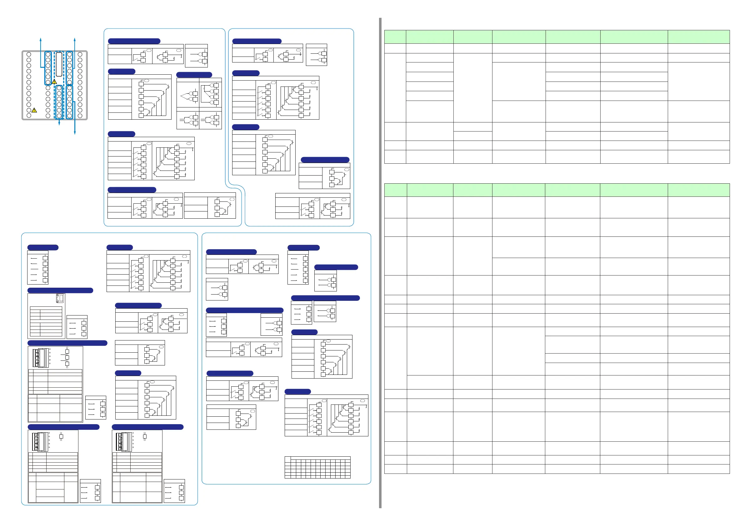
E1-Terminal Area
301-306
E2-Terminal Area
307-312
(Optional suffix code /X1)
Contact input
External contact input
DI11
DI12
DI13
DI14
DI15
COM
Common
DI11
DI12
COM
+5V
+5V
No-voltage contact
Transistor contact
Contact rating: 12 V DC, 10 mA or more
DI13
+5V
DI14
+5V
DI15
+5V
Factory default: No function
Factory default: No function
Factory default: No function
Factory default: No function
Factory default: No function
UP UP
301
302
303
304
305
306
301
302
303
304
305
306
Function can be assigned to the terminals with no function.
DI
Contact output
External contact output (transistor)
Transistor contact rating: 24 V DC, 50 mA
DO12
DO11
DO13
DO14
DO15
COM
Common
UP
(Optional suffix code /Y1)
PV event-4 output
PV event-5 output
PV event-6 output
PV event-7 output
PV event-8 output
301
302
303
304
305
306
Function can be assigned to the terminal with no function.
DO
(Optional suffix code /U1)
Universal input
TC input RTD input
Voltage (mV, V) input
+
-
+
-
Current (mA) input
+
-
4-wire
302
303
302
303
303
304
RSP
a
B
b
A
301
302
303
305
(Optional suffix code /R1)
Remote input / Contact input
External contact input
DI16
COM
Common
DI16
COM
+5V
No-voltage contact
Transistor contact
Contact rating: 12 V DC, 10 mA or more
UP UP
Start of remote-mode
operation when DI16
switches from OFF to ON.
303
304
303
304
RSP
Remote input
Default: 1-5 V DC
+
-
305
306
Specify within a
range of 1-5 V DC,
0-2 V DC,0-10 V DC
Contact output
External contact output
Transistor contact rating: 24 V DC, 50 mA
DO22
DO21
DO23
DO24
DO25
COM
Common
UP
(Optional suffix code /Y2)
307
308
309
310
311
312
Function can be changed.
DO
Time event-5 output
Time event-4 output
Time event-3 output
Time event-2 output
Time event-1 output
(Optional suffix code /W1)
External contact output
Transistor contact rating: 24 V DC, 50 mA
DO12
DO11
COM
Common
UP
Contact input / Contact output
External contact input
DI11
DI12
COM
Common
No-voltage contact
Transistor contact
Contact rating: 12 V DC, 10 mA or more
Factory default: No function
Factory default: No function
UP
301
302
303
304
305
306
DI/DO
Function can be assigned to the terminals with no function.
DI11
DI12
COM
+5V
+5V
UP
301
302
303
(Optional suffix code /X2)
Contact input
External contact input
DI21
DI22
DI23
DI24
DI25
COM
Common
DI21
DI22
COM
+5V
+5V
No-voltage contact
Transistor contact
Contact rating: 12 V DC, 10 mA or more
DI23
+5V
DI24
+5V
DI25
+5V
Factory default: No function
Factory default: No function
Factory default: No function
Factory default: No function
Factory default: No function
UP UP
307
308
309
310
311
312
307
308
309
310
311
312
Function can be assigned
to the terminals with no
function.
DI
(Optional suffix code /W2)
External contact output
Transistor contact rating: 24 V DC, 50 mA
DO22
DO21
COM
Common
UP
Contact input / Contact output
External contact input
DI21
DI22
COM
Common
DI21
DI22
COM
+5V
+5V
No-voltage contact
Transistor contact
Contact rating: 12 V DC, 10 mA or more
Factory default: No function
Factory default: No function
UP UP
307
308
309
307
308
309
310
311
312
DI/DO
Function can be
assigned to the
terminals with no
function.
(Optional suffix code /A2)
Aux. analog input
Default: 1-5 V DC
+
-
Aux. analog input / Contact input
External contact input
DI26
COM
Common
DI26
COM
+5V
No-voltage contact
Transistor contact
Contact rating: 12 V DC, 10 mA or more
Factory default: No function
UP UP
309
310
309
310
311
312
Function can be assigned to the terminals with no function.
AIN2
Specify within a
range of 1-5 V DC,
0-2 V DC,0-10 V DC
PV event-4 output
PV event-5 output
Time event-1 output
Time event-2 output
E3-Terminal Area
401-412
E4-Terminal Area
501-506
(Optional suffix code /ET3)
Ethernet communication (with gateway function)
10BASE-T/100BASE-TX
RJ45 connector
Color
Lit
Unlit
Amber
100M bps
10M bps
Green
Linked
Active
Link failure
Color
Lit
Blink
Unlit
Upper side LED (baud rate)
Lower side LED (link activity)
RS-485
RSB(+)
RSA(-)
SG
407
408
409
ETHR
RS-485
SDB(+)
SDA(-)
RDB(+)
RDA(-)
SG
RS-485 communication
(Optional suffix code /CH3)
407
408
409
410
411
RS485
Contact input
External contact input
DI41
DI42
DI43
DI44
DI45
COM
DI41
DI42
COM
+5V
+5V
DI43
+5V
DI44
+5V
DI45
+5V
UP UP
(Optional suffix code /X4)
Common
No-voltage contact
Transistor contact
Contact rating: 12 V DC, 10 mA or more
Bit-0 of
program pattern number
Bit-1 of
program pattern number
Bit-2 of
program pattern number
Bit-3 of
program pattern number
Bit-4 of
program pattern number
501
502
503
504
505
506
501
502
503
504
505
506
Function can be changed.
DI
(Optional suffix code /X3)
Contact input
External contact input
DI31
DI32
DI33
DI34
DI35
COM
Common
DI31
DI32
COM
+5V
+5V
No-voltage contact
Transistor contact
Contact rating: 12 V DC, 10 mA or more
DI33
+5V
DI34
+5V
DI35
+5V
Factory default: No function
Factory default: No function
Factory default: No function
Factory default: No function
Factory default: No function
UP UP
407
408
409
410
411
412
407
408
409
410
411
412
DI
Function can be assigned to the terminals with no function.
Contact output
(Optional suffix code /Y3)
DO
External contact output
DO32
DO31
DO33
DO34
DO35
COM
Time event-6 output
Time event-7 output
Time event-8 output
Time event-9 output
Time event-10 output
Common
UP
407
408
409
410
411
412
Transistor contact rating: 24 V DC, 50 mA
Function can be changed.
RS-485
SDB(+)
SDA(-)
RDB(+)
RDA(-)
SG
RS-485 communication
501
502
503
504
505
RS485
(Optional suffix code /C4)
RS-485
RSB(+)
RSA(-)
SG
RS
-
485 communication/24 V DC loop power supply
+
24 V DC loop power supply
21.6-28.0 V DC
(Max. 30 mA DC)
-
501
502
503
505
506
RS485/LPS24
(Optional suffix code /LC4)
+
24 V DC loop power supply
21.6-28.0 V DC
(Max. 30 mA DC)
-
24 V DC loop power supply
505
506
LPS24
(Optional suffix code /L4)
Aux. analog input/Contact input
(Optional suffix code /A4)
AIN4
Aux. analog input
Default: 1-5 V DC
+
-
External contact input
DI46
COM
DI46
COM
+5V
UP UP
Common
No-voltage contact
Transistor contact
Contact rating: 12 V DC, 10 mA or more
Factory default: No function
503
504
503
504
505
506
Function can be assigned to the
terminals with no function.
Specify within a
range of 1-5 V DC,
0-2 V DC,0-10 V DC
(Optional suffix code /PD3)
PROFIBUS-DP communication (with Modbus master)
Pin
1
2
Signal name Description
VP
RxD/TxD-P
3 RxD/TxD-N
4
DGND
5
SHIELD
+5V bus power
Data signal
(positive data receive/transmit)
Data signal
(negative data recive/transmit)
Signal ground
Shield ground
RS-485
RSB(+)
RSA(-)
SG
407
408
409
PROF
If the UP is located at the
end of a segment for the
PROFIBUS
communication wiring,
terminating resistors are
separately needed.
These are to be prepared
by users. (390 Ω: 2 pcs.
220 Ω: 1 pc., or an active
terminator.)
VP
RxD/TxD-P
Data
line
Data
line
390Ω
220Ω
390Ω
RxD/TxD-N
DGND
LED
CHK
(red)
RDY
(green)
Lit
Unlit
ERR
(red)
User profile error
CHK
RDY
ERR
1
2
3
4
5
Normal
Normal
Not connected, or
communication
failure (flashing)
Normal.
Communicating
successfully
No electricity, or
communication
failure
Contact output
External contact output
DO42
DO41
DO43
DO44
DO45
COM
Factory default: No function
Factory default: No function
Factory default: No function
Factory default: No function
Factory default: No function
Common
UP
(Optional suffix code /Y4)
501
502
503
504
505
506
DO
Transistor contact rating: 24 V DC, 50 mA
Function can be assigned to the
terminals with no function.
(Optional suffix code /W4)
Contact input / Contact output
DI/DO
External contact output
Transistor contact rating: 24 V DC, 50 mA
DO42
DO41
COM
Common
UP
External contact input
DI41
DI42
COM
Common
No-voltage contact
Transistor contact
Contact rating: 12 V DC, 10 mA or more
Factory default: No function
Factory default: No function
UP
501
502
503
504
505
506
Function can be assigned to the terminals with no function.
DI41
DI42
COM
+5V
+5V
UP
501
502
503
RS-485 communication / Aux. analog input / Contact input
(Optional suffix code /AC4)
External contact input
DI46
COM
Common
DI46
COM
+5V
No-voltage contact
Transistor contact
Contact rating: 12 V DC, 10 mA or more
UP UP
Factory default: No function
503
504
503
504
AIN4/RS485
Aux. analog input
Default: 1-5 V DC
+
-
505
506
Specify within a
range of 1-5 V DC,
0-2 V DC,0-10 V DC
RS-485
RSB(+)
RSA(-)
SG
501
502
503
Program pattern number
1 2 3 4 5 6 7 8 9 10 11 12
DI41 ON OFF ON OFF ON OFF ON OFF ON OFF ON OFF
DI42 OFF ON ON OFF OFF ON ON OFF OFF ON ON OFF
DI43 OFF OFF OFF ON ON ON ON OFF OFF OFF OFF ON
DI44 OFF OFF OFF OFF OFF OFF OFF ON ON ON ON ON
DI45 OFF OFF OFF OFF OFF OFF OFF OFF OFF OFF OFF OFF
(Suffix code: Type 3=5,
except Type 2=3)
DeviceNet communication (with Modbus master)
RS-485
RSB(+)
RSA(-)
SG
407
408
409
DNET
If the UP is located at
the end of a segment
for the DeviceNet
communication wiring,
terminating resistors
are separately needed.
These are to be
prepared by users.
(121 Ω: 1 pc.)
CAN_H
CAN_L
121Ω
LED
CHK
(red)
RDY
(green/
red)
Lit/flashing
Unlit
User profile error
Normal
Pin
1
2
Signal name Description
CAN_H
CAN_L
3
V+
4
V-
5
DRAIN
RX/TX + signal
RX/TX - signal
Shield/Drain wire
DeviceNet power supply 24V
DeviceNet power supply common
Normal. Communicating
successfully (green, lit).
Not connected (green, flashing).
Critical link failure (red, lit).
Communication timeout (red,
flashing)
At power-on/Communication
faulted (green/red, flashing)
No electricity
CHK
MNS
1
2
3
4
5
(Suffix code: Type 3=3,
except Type 2=3)
CC-Link communication (with Modbus master)
RS-485
RSB(+)
RSA(-)
SG
407
408
409
CC-L
If the UP is located at
the end of a segment
for the CC-Link
communication wiring,
terminating resistors
are separately needed.
These are to be
prepared by users.
(110 Ω: 1 pc.)
DA
DB
110Ω
LED
CHK
(red)
L ERR
(red)
L RUN
(green)
Lit
Unlit
User profile error
Normal
Normal
Pin
1
2
Signal name Description
DA
DB
3 DG
4
SLD
5
FG
RX/TX - signal
RX/TX + signal
Frame ground
TX/RX signal ground
Shield
Normal
Communicating successfully
Communication failure
(CRC error)
No carrier
detected/
Connection
timeout
CHK
L RUN
L ERR
1
2
3
4
5
Function can be assigned to the terminals with no function.
(Optional suffix code /W3)
Contact input / Contact output
External contact input
DI31
DI32
COM
Common
No-voltage contact
Transistor contact
Contact rating: 12 V DC, 10 mA or more
Factory default: No function
Factory default: No function
UP
407
408
409
DI/DO
DI31
DI32
COM
+5V
+5V
UP
407
408
409
External contact output
Transistor contact rating: 24 V DC, 50 mA
DO32
DO31
COM
Common
UP
410
411
412
Time event-6 output
Time event-7 output
A program pattern is selected with the combination of ON and OFF of a
contact input.
In the case of a pattern 5, ON (1) of "DI45 to DI41" and OFF (0) is
represented as a binary number "00101": it is "5" decimally.
The pattern 13 or later can be selected similarly.
Bit-0 of
program pattern number
Bit-1 of
program pattern number
E4-terminal area
E3-terminal area
E2-terminal area
E1-terminal area
101
102
103
104
105
106
107
108
109
110
111
501
502
503
504
505
506
507
508
509
510
511
512
407
401
408
409
410
411
412
301
302
303
304
305
306
307
308
309
310
311
312
201
202
203
204
205
206
207
208
209
210
211
212
101
-112
501
-512
401
-412
301
-312
201
-212
112
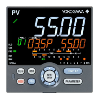
■ UP55A(Continuedfrompage3) [ Operations 13. Troubleshooting ]
n
Errors at Power On
Theerrorsshownbelowmayoccurinthefaultdiagnosiswhenthepoweristurnedon.(FordetailsofSetpointdisplayandinput/outputactionwheneacherroroccurs,seeUser’sManual.
PV display
(Operation
Display)
Setpoint display
(Operation Display)
Status indicator
(Operation Display)
Parameter that displays error
details
Error description Cause and diagnosis Remedy
Indication of
f Indication off — — FaultyMCU
RAM/MCUROM MCURAM/MCUROMarefailed.
Faulty.
Contactusforrepair.
ERR
SYS-----
—
— System data
error System data is corrupted.
Faulty.
Contactusforrepair.
PAR0004
(foruserdefaultvalueerroronly)
Setupparameter(PA.ER)
User(parameter)defaultvalue
error
Userparameter
iscorrupted.
Initializedtofactorydefaultvalue.
Checkandreconguretheinitialized
settingparameters.Errorindicationis
erased when the power is turned on
again.
PAR0010
(forsetupparametererroronly)
Setup parameter error
Setup parameter data is corrupted.
Initializedtouserdefaultvalue.
PAR0020
(foroperationparametererroronly)
Operationparametererror
Operationparameterdataiscorrupted.
Initializedtouserdefaultvalue.
PAR0040
(forprogrampatternerroronly)
Programpatternerror
Programpatterndataiscorrupted.
Allprogrampatternsaredeleted.
SLOT0017
(0017:Erroroccurstoall
hardwareofE1toE4-terminal
areas.)
Setupparameter
(OP.ER)
Nonrespondinghardwareof
extendedfunction(E1toE4-
terminalareas)
Inconsistence of system data and
hardwareofextendedfunction.
Nonrespondingcommunicationbetween
hardwareofextendedfunction(E1toE4-
terminalareas).
Faulty.
Contactus
forrepair.
Normal
indication
Normalindication
Rightmost
decimalpoint
onPVdisplayblinks.
Setupparameter(PA.ER)
Calibrationvalueerror
Initializedtocalibrateddefaultvaluebecause
ofcorruptedfactorydefaultvalue.
Faulty.
Contactusforrepair.
Rightmostdecimalpoint
onSymboldisplayblinks.
FaultyFRAM
Datawriting(storing)toFRAMisimpossible.
Normal
indication
Normalindication LADDER
lampblinks Setupparameter(LA.ER) Corruptedladderprogram
Ladderprogramiscorrupted.
Operateswithoutladderprogram.
Downloadtheladderprogramagain.
Normal
indication
0.00000000
(Decimalpointontheleftof
theSymboldisplayblinks)
— Setupparameter
(OP.ER) Userproleerror Userproleiscorrupted. Downloadtheuserproleagain.
[ Operations 13. Troubleshooting ]
n
Errors during Operation
Theerrorsshownbelowmayoccurduringoperation.(Forinput/outputactionwheneacherroroccurs,seeUser’sManual.
PV display
(Operation
Display)
Setpoint display
(Operation Display)
Status indicator
(Operation Display)
Parameter that displays
error details
Error description Cause and diagnosis Remedy
AD.ERR
Normalindication(Note) — Setupparameter(AD1.E)
AnaloginputterminalADCerror
•PVinput
•RSPinput(E1-terminalarea)
•AIN2input(E2-terminalarea)
•AIN4input(E4-terminalarea)
AnaloginputterminalADvalueerror
Faulty.
Contactus
forrepair.
RJC.E
(DisplaysRJC.
EandPV
alternately.)
Normalindication(Note) — Setupparameter(AD1.E)
UniversalinputterminalRJCerror
•PVinput
•RSPinput(E1-terminalarea)
UniversalinputterminalRJCerror
Faulty.
Contactus
forrepair.
SettheparameterRJCtoOFFtoerase
error indication.
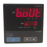
B.OUT
Normalindication(Note) —
Setupparameter(AD1.E)
Analoginputterminalburnouterror
•PVinput
•RSPinput(E1-terminalarea)
•AIN2input(E2-terminalarea)
•AIN4input(E4-terminalarea)
Analoginputterminalsensorburnout
Checkwiringandsensor.
Errorindicationiserasedinnormal
operation.
Set
upparameter(PV1.E/PV2.E)
PVinputburnouterror(Loop1,
Loop2)
BurnoutofanaloginputconnectedtoPV
Checkwiringandsensorofconnected
analoginputterminals.
Errorindicationiserasedinnormal
operation.
OVER
-OVER
Normalindication — Setupparameter(PV1.E/PV2.E)
PVinputover-scale
PVinputunder-scale
(PVvaluesoutof-5to105%)(Loop
1,Loop2)
PVinputisoutof-5to105%.Alsooccurs
whenthedataoutofrangewhichisthe
ladder calculation result is input.
Checkanaloginputvalueorladder
program.
Normal
indication
Normalindication — Setupparameter
(PV1.E) RSPinputburnouterror(Loop1) BurnoutofanaloginputconnectedtoRSP
Checkwiringandsensor.Error
indication is erased in normal operation.
Normal
indication
RSPB.OUT
— Setupparameter(PV1.E)
BurnouterrorwhenRSPinputis
usedforcontrol(Loop1)
BurnoutofanaloginputconnectedtoRSP
whenRSPisusedforcontrolcomputation
Checkwiringandsensor.Error
indication is erased in normal operation.
Normal
indication
OUT-----
— Setupparameter(AD2.E)
Feedbackinputresistor/current
burnout
Feedbackinput
burnout
Checkwiringoffeedbackinputresistor/
current.Errorindicationiserasedin
normal operation.
Normal
indication
Normalindication LADDER
lampblinks Setupparameter(LA.ER)
Laddercalculationoverow
Floatingpointcomputationforladder
calculationisinnite.
Checktheladderprogram.
Loadfactorover100%
Computationdoesnotendwithinthe
controlperiod.(Whentheloadfactoris
100%ormore,andthecomputationdoes
notendwithinthecontrolperiod.)
Changethecontrolperiodorreduce
thenumberofstepsfortheladder
program.
Loadfactor
over200%
(Forcedend)
Computationdoesnotendwithinthecontrol
period(loadfactoris200%ormore).
Changethecontrolperiodorreducethe
numberofstepsfortheladderprogram.
Ladderprogramerror Ladderprogramiscorrupted.
Downloadtheladderprogramagain.If
the error indication is still not erased,
thereisafault.Contactusforrepair.
0.00000000
(Decimalpointontheleftof
theSymboldisplayblinks)
— Setupparameter(OP.ER) Peer-to-peercommunicationerror Peer-to-peercommunicationerror
Checkthatthetargetdevicesare
connected correctly.
Recoveryatnormalreceipt.
AT.E
Normalindication — Setupparameter(PV1.E/PV2.E)
Auto-tuningtime-out
(Loop1,Loop2)
Auto-tuningdoesnotendevenwhen24
hourshaveelapsedafterthestartoftuning.
Checktheprocess.Holddownanykeyto
erase the error indication
VAT.E
Normalindication — Setupparameter(AD2.E)
Valvepositionautomatic
adjustmenterror
Fully-closedvalvepositionisequaltoorlarger
thanthefully-openvalvepositionafterautomatic
valvepositionadjustmentisperformed.
Checkwiringandvalve.Holddownany
key to erase the error indication.
Normal
indication
0.00000000
(Decimalpointontheleftof
theSymboldisplayblinks)
— Setupparameter
(OP.ER)
Communicationerror
(RS-485communication)
Framingparityerror
Bufferoverow
Inter-charactertime-out
Checksumerror(PClinkcommunicationwith
checksum)
CRCcheckerror(Modbus/RTU)
LRCcheckerror(Modbus/ASCII)
Checkthecommunicationparameters.
Recoveryatnormalreceipt.
Holddownanykeytostopblinking.
Normal
indication
0.00000000
(Decimalpointontheleftof
theSymboldisplayblinks)
— Setupparameter
(OP.ER) Userproleerror Userproleiscorrupted. Downloadtheuserproleagain.
Normal
indication
Normalindication
Rightmostdecimalpointon
Symboldisplayblinks.
Setupparameter(PA.ER) FaultyFRAM
Writing(storing)datatoFRAMisimpossible.
Faulty.Contactusforrepair.
Undened Undened — —
FaultyMCU
/DCU
(ROM/RAMerror,corrupted)
MCU/DCUiscorrupted. Faulty.Contactusforrepair.
Note:WhenanerroroccursininputshowninAnaloginputdisplay(Operationdisplay),SetpointdisplayshowsthesamesymbolasthePVdisplay.
 Loading...