THEORY OF OPERATION
3. THEORY OF OPERATION
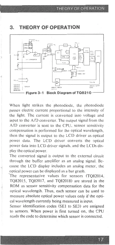
Figure 3-1 Block Diagram of T08210
When light strikes the photodiode, the photodiode
passes electric current proportional to the intensity of
the light. The current is converted into voltage and
input to the A/D converter. The output signal from the
A/D converter is sent to the CPU, sensor sensitivity
compensation is performed for the optical wavelength,
then the signal is output to the LCD driver as optical
power data. The LCD driver converts the optical
power data into LCD driver signals, and the LCDs dis-
play the optical power.
The converted signal is output to the external circuit
through the buffer amplifier as an analog signal. Be-
cause the LCD display includes an analog meter, the
optical power can be displayed as a bar graph.
The representative values for sensors (TQ82014,
TQ82015, TQ82017, and TQ82018) are stored in the
ROM as sensor sensitivity compensation data for the
optical wavelength. Thus, each sensor can be used to
measure absolute optical power values only if the opti-
cal wavelength currently being measured is input.
Sensor identification codes (SE! to SE3) are assigned
to sensors. When power is first turned on, the CPU
reads the code to determine which sensor is connected.
17
 Loading...