4.
EXPLANATION OF EACH OPERATING PRINCIPLES
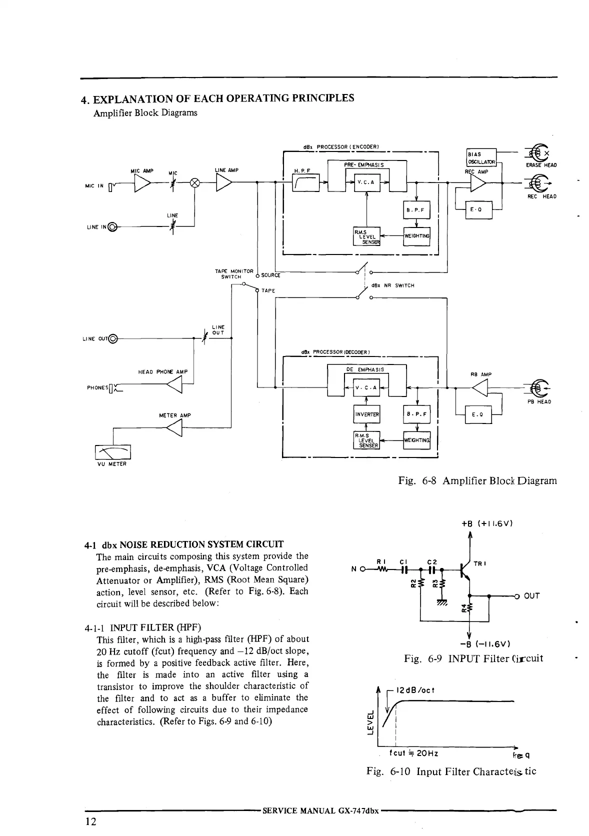
Amplifier Block Diagrams
MIC
IN
ov-{>-!•---"-"------'
TAPE
MONITOR
SWITCH
SOURCE
f
LINE
OUT
LINE
OUT(Qt---------.-
HEAD
PHO!£ AMP
METER
AMP
VU
METER
TAPE
.
L
__
4-1
dbx
NOISE
REDUCTION
SYSTEM
CIRCUIT
=v
ERASE
HEAD
~~
REC
HEAD
dBx
NR
SWITCH
RB
AMP
PB
HEAD
Fig.
6-8
Amplifier Block Diagram
+B
(+I
l,6V)
RI
Cl
The main circuits composing this system provide the
pre-emphasis, de-emphasis,
VCA
(Voltage Controlled
Attenuator or Amplifier),
RMS
(Root Mean Square)
action, level sensor, etc. (Refer to Fig. 6-8). Each
circuit
will
be
described below:
N
~
TRI
4-1-1
INPUT FILTER (HPF)
This filter, which
is
a high-pass filter (HPF)
of
about
20
Hz
cutoff (fcut) frequency and
-12
dB/oct slope,
is
formed by a positive feedback active filter. Here,
the filter
is
made into an active filter using a
transistor to improve the shoulder characteristic
of
the filter and
to
act
as
a buffer to eliminate the
effect
of
following circuits due to their impedance
characteristics. (Refer to Figs.
6-9
and 6-10)
..,.
er
.--->---o OUT
-B
H
l,6Vl
Fig. 6-9 INPUT Filter Circuit
[
12d8/oct
g
Yf
~
I
I
fcut::;
20Hz
Fig. 6-10 Input Filter Charactelis tic
----------------
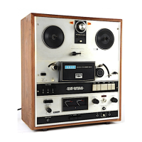
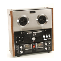
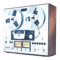
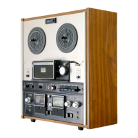
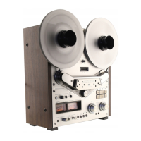
SERVICE MANUAL GX-747dhx
----------------
12
 Loading...