4.
dbx NR
PC
BOARD ADJUSTMENT
NOTICES
capacitor 10/25V).
i
1.
Adjustment
of
the dbx NR
is
not required except
when a
part
is
replaced or an adjustable VR
is
turned
by
mistake.
2. Since an
error
will be caused in the zero point
level and detected time constant, when the dbx
NR
power supply voltage
is
not normal, be sure
to adjust accurately.
3.
Be
specially cautious for the replacement
of
R22,
R49 (22
M ohms), C17, and
C33
(tantalum
0 0
Since the values
of
R22 and R49
are
as
high
as
22
Mohms,
be
cautious about dirt, flux, frost, etc.
When
C
17
and
C33
of
small dielectric strength
are
used, misoperation can sometimes occur due to a
change in leakage current.
4.
In R.M.S symmetry adjustment (step 2), Observe
the signals at the testpoints
(TP
3 to
TP
6) by
refering to Fig. 9-8. Due
to
the signals at those
testpoints are very low level.
o 0
8
~~
l!Jo
-:i~
LIN
RCH
LCH
RIN
RCH
LCH VR3b VR3
LOUT
~
0 0 n n
0001C4nr
I.
no
I ROUT
TP6~
,c,
VRlbo
v.,
,c,u~TP5
TP4~
LJ'c•
u y "
J~~::
1
i
r.n
y:xJ
15tt
L
OUT
•~~c
2
,ca
,c~~"
Ic•
,cs
,c:~H
c=G::'.~::'.:cD:'.:
7
=::i
R
ouT
RCH
VR2b
VR5b
00
0
VR I
ENCODER
V.C.A SYMMETRY
VR2
ENCODER
R.M.S SYMMETRY
VR3
DECODER
V.C.A SYMMETRY
VR4
DECODER
R.M.S SYMMETRY
VR5
ENCODER
ZERO POINT
VR6
DECODER
ZERO POINT
VR7
POWER
SUPPLY
LCH
RCH
00~
VR5 VR2 VR4b VR6b
i- VRlb
to
VR6b
IS
l
NDICATE
RIGHT
CHANNEL
·X·
EACH
TEST POINT
IS
USEING
. JUMPER RESISTER
Fig. 9-6
dbx
Noise
Reduction
P.C.
Board
Adjustment
point
&
Test
point
STEP
ADnJSTMENT
INPUT SIGNAL • TEST POINT i ADJUSTMENT
RESULT
RE!v.1ARKS
ITEM
• • POINT
I
I
Adjust
so
that
TP-1
out-
TPI VR7
10KB
put voltage becomes
Power Supply
±11.6±0.IV.At
this
See
l'.'lote 2.
I
time, make sure that
TP2
TP-2
voltage
is
within
I
-11.6±0.4V.
•
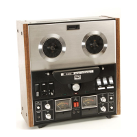
---------------SERVICE
MANUAL
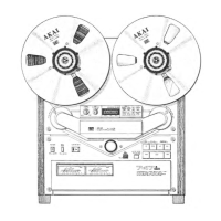
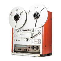
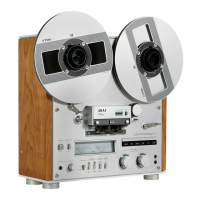
GX-747dbx
---------------
39
 Loading...