4-1-3
DE-EMPHASIS CIRCUIT (Figs. 6-12 and 6-13)
In
contrast
to
the pre-emphasis circuit which pre-
emphasizes the high frequency band during recording,
this circuit de-emphasizes the high frequency band
during playback to restore the
signal
to its original
4-14
VCA
(Voltage Controlled Amplifier (or At-
tenuator)) CIRCUIT (Refer to Figs. 6-14,6-15,6-16)
.---------
+ B (
+11,6
VJ
'---+-------+---
-B
(-11,SV)
From R,M.S
Sencor
Fig. 6-14 Encoder
GND
I
set
Vee
GAIN
CELL
IDLING
CURRENT SUPPLY
GC
I
I out
GC
3
Fig. 6-16
IC
µPC1252H2 Internal Block Diagram
ICl and
IC4
(µPC1252H2)
are
dbx
VCA
circuit
ICs.
Pin
(D
is
a virtual ground, and accepts only
an
input
signal
current.
Pin
@
is
a
high
impedance current
output.
Fig. 6-13 De-emphasis Circuit
state. The circuit configuration
is
the
same
as
the
pre-emphasis circuit, but
has
some differences in
component values.
INPUT
.--------,;.
+9
(+11,SV)
1-----<;;
OUTPUT
L......---1-------B
(-11.SV)
From
R.M.S
Sencor
Fig.
6-1
S
Decoder
Pin
~
is
connected to negative power supply through
the current setting internal bias circuit. The set
current
is
nominally 2 mA. The range
is
co:rnpressed
in the encode mode when the
RMS
sens~r
cutput
is
positive. In the decode mode,
since
the
RN.IS
sensor
output
is
fed
to Pin
a)
with
Pin
@ beini
GND,
the
range
is
expanded when the
RMS
sensor
output
is
positive, and it
is
compressed when the
MS
sensor
output
is
negative, which
is
just the opposi 1e action
to the encode mode.
The circuit consisting of R9(R37),
Rl0[R.38), and
VRl
(VR3) can make symmetrical adjusiroent
pos-
sible
and minimize
DC
offset voltage
-..Nhich
is
multiplied by the circuit gain, and controlth.e second
order harmonic distortion.
When
a fast
gain
4;:hange
is
commanded,
DC
offset appears
at
the
Oiltj)Ut.
R8
(R36)
are
provided to reduce this. In
tie
encoder
(Fig. 6-14), it acts
as
a logarithmic amplifier, while
it acts
as
an
anti-logarithmic amplifier in
ie
decoder
(Fig. 6-15). Fig. 6-16
shows
IC
µPC125lff2 block
diagram.
----------------
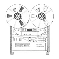
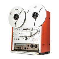
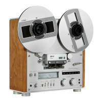
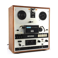
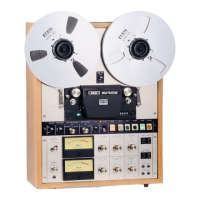
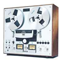
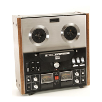
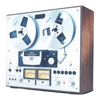
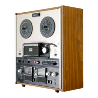
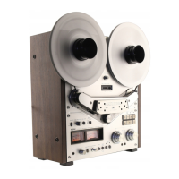
SERVICE MANUAL GX-747dbx
----------------
14
 Loading...