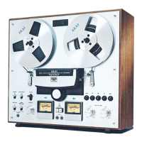
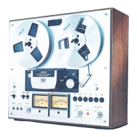
4-1-7
RMS
(ROOT
MEAN
SQUARE) LEVEL SENSOR
(Figs.
6-21
and 6-22)
R22 22M
,-....,1--<1,__
__
+BC+
11.6V
l
....._
______________
-BC-ll.6Vl
Fig.
6-21
RMS
Level Sensor Circuit
Vee
SQUARELAW
AMPLIFIER
)-----16
)---------'
Vee Is
CAP.
Fig. 6-22
IC
µPC1253H2 Block Diagram
The
RMS
level sensor circuit detects the effective
value (RMS)
of
input signal current, and converts it
to a
DC
voltage proportional to the logarithm
of
the
detected level.
IC2
and
IC5
(µPC1253H2)
are
for the dbx
RMS
level
sensor circuit.
Fig.
6-21
shows the
RMS
level
sensor circuit. For
pre-setting the control
signal
(OV
at zero point level)
for the input level, zero point level control
is
made
possible by varying the operating current
of
IC
by
means
of
YRS. (Zero point level=410 mV=-5.5
dB
ref
lmW
600 ohms (0.774 volts))
The attack time
is
15
ms
when there
is
a
IO
dB
level
change (increase),
5
ms
when there
is
a 20
dB
change,
and 3
ms
when there
is
a 30
dB
change. The decay
rate (Note 2)
is
125
dB/sec
as
standard. Time
constant
is
determined by the current
(11)
flowing
through R26, and by
Cl
7.
In
the GX-747 dbx,
since
IT=7.5 µA, in
the
equation
for obtaining the decay rate
of
125
dB/sec, C=IOµF
from IT=0.75
C.
Cl8
is
a by-pass capacitor, and the charging iurrent
of
Cl7
flows through Cl8.
Cl6
is
a capacitorprovided
to obtain stability and low distortion chanc1:eristics
in the high frequency band.
R25
serves
as
ale'-'el shift
for bringing the control
value
to
the
center. VR2
is
a volume control for symmetry adjustment.
R22 prevents any ''thump" sound when
tle~e
is
no
signal.
Note 2. Slope
of
the output
voltage
change a.Jter an
abrupt
large
drop
of
the input signal lere
1.
Note 3.
GND
is used for common,
othenise
mis-
operation may result due to the
larl,'!
current
flowing during the recovery time.
---------------SERVICE
MANUAL
GX-747dbx---------------
16
 Loading...