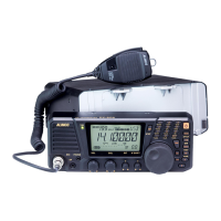
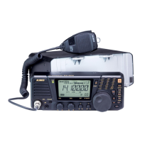
Do you have a question about the Alinco DX-70 and is the answer not in the manual?
Details general operating parameters like mode, channels, impedance, power, temperature, and dimensions.
Covers transmitter frequency coverage, power output for different bands, and modulation systems.
Outlines receiver circuitry, frequency range, intermediate frequencies, sensitivity, and selectivity.
Explains the signal path and components within the receiver system, including antenna inputs and filter units.
Details the front-end stages of the receiver, including filtering, amplification, and signal processing.
Describes the microphone amplifier, balanced mixer, and IF filters for the transmitter system.
Covers the power amplifier stages, including final stage amplification and fan control.
Describes the function and operation of the main power switch.
Explains the regulated power supplies for the CPU and other circuits.
Details the circuit responsible for controlling the LCD brightness.
Describes the LCD display indications and driver.
Covers miscellaneous front unit functions and indicators.
Provides a brief overview of the PLL unit's functions, including signal generation and power supply.
Explains the specific power supplies, frequency generation, and mode-dependent signal processing within the PLL unit.
Provides block diagram and electrical data for the tone generator IC.
Details the low-power FM IF IC, including its block diagram and specifications.
Presents the block diagram and characteristics of the dual operational amplifier IC.
Shows the pinout and function of the 8V voltage regulator IC.
Provides test circuit and pinout for the audio power amplifier IC.
Details the 8V voltage regulator IC, including its input/output pins.
Lists pin names and descriptions for the 8-bit serial-in/parallel-out driver IC.
Shows the block diagram and truth table for the bilateral switch IC.
Presents the block diagram for the dual operational amplifier IC.
Details the logic diagram and truth table for the analog multiplexer/demultiplexer.
Provides the truth table and block diagram for the 8-stage shift register IC.
Shows the block diagram and characteristics of the two-modulus prescaler IC.
Presents the block diagram and truth table for the 12-stage binary ripple counter.
Details the block diagram and truth table for the dual ripple counter IC.
Shows the block diagram and truth table for the 7-stage binary counter IC.
Provides the truth table for the quad 2-input OR gate IC.
Presents the pinout and block diagram for the PLL frequency synthesizer IC.
Details the pinout and block diagram for the PLL frequency synthesizer IC.
Shows the truth table and pinout for the quad 2-input NOR gate IC.
Provides parameter ratings and test circuit for the balanced modulator IC.
Details parameters and test circuit for the low voltage dual VCA IC.
Shows pin names and descriptions for the LCD driver IC.
Presents parameters and test circuit for the FM front end IC.
Shows the truth table for the dual D-type flip flop IC.
Details the block diagram and parameters for the voltage regulator IC.
Shows the pinout for the 5V voltage regulator IC.
Provides the truth table and pinout for the quad exclusive-OR gate IC.
Details the block diagram and pin names for the serial EEPROM IC.
Presents parameters and block diagram for the double balanced modulator IC.
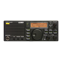
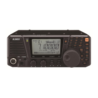
Illustrates the front panel components and layout of the EDX-1.
Details the disassembly and assembly of the second front control unit.
Illustrates the components and assembly of the LCD unit.
Shows the exploded view of the PLL unit and fan assembly.
Depicts the internal layout and component placement from the top view.
Shows another perspective of the internal layout and component placement.
Illustrates the components and assembly of the LPF unit.
Details the exploded view of the PA unit and its connection to the LPF unit.
Lists all parts and their descriptions for the main unit of the device.
Lists parts specific to the BPF3 unit.
Lists parts specific to the BPF4 unit.
Lists parts specific to the BPF5 unit.
Lists connectors used in the device.
Lists parts for the microphone unit.
Lists parts for the PLL unit, covering various sub-circuits.
Lists parts for the VCO2 and VCO3 units.
Lists parts for VCO3, NFB, TONE, and FILT units.
Lists parts for the FILT unit.
Lists parts for the FILT and PA units.
Lists parts for the power amplifier unit.
Lists parts for PA unit, jacks, and front panel components.
Lists parts associated with the front panel of the device.
Lists screws, holders, knobs, and other mechanical components.
Lists packing materials and related accessories.
Details test equipment and points for adjusting the PA unit.
Describes how to set the idle current for the PA unit.
Explains the procedure for adjusting the SWR of the transmitter.
Provides specific steps for adjusting PA unit parameters like idling current and output power.
Covers test equipment and points for adjusting the PLL unit.
Details how to adjust the tone frequency and level for FM transmission.
Identifies specific adjustment points on the main unit's circuit board.
Procedures for adjusting receiver sensitivity across different bands and modes.
Procedure for adjusting the noise blanker circuit for optimal performance.
Details the procedure for calibrating the S meter and squelch.
Covers adjusting Automatic Gain Control (AGC) for optimal receiving.
Outlines required test equipment and setup for transmission adjustments.
Procedures for tuning transmitter output power, current limit, and FM deviation.
Steps to minimize spurious emissions and balance carrier signals.
Shows component layout for the CPU unit, side A.
Shows component layout for the CPU unit, side B.
Component layout for the volume control unit, side A.
Component layout for the volume control unit, side B.
Component layout for the jack unit, side A.
Component layout for the jack unit, side B.
Shows component layout for the main unit, side A.
Shows component layout for the main unit, side B.
Component layout for the power amplifier unit, side A.
Component layout for the power amplifier unit, side B.
Component layout for the filter unit, side A.
Component layout for the filter unit, side B.
Component layout for the PLL unit, side A.
Component layout for the PLL unit, side B.
| Modes | SSB, CW, AM, FM |
|---|---|
| Impedance | 50 ohms |
| Supply Voltage | 13.8 V DC ±15% |
| Power Output | 100 W (SSB, CW), 40 W (AM) |
| Current Drain | 20 A |
| Selectivity | SSB: 2.4 kHz (-6 dB), 4.5 kHz (-60 dB) |