16 / 31
ZYNQ FPGA Development Platform AC7015 User Manual
Amazon Store: https://www.amazon.com/alinx
Sales Email: rachel.zhou@aithtech.com
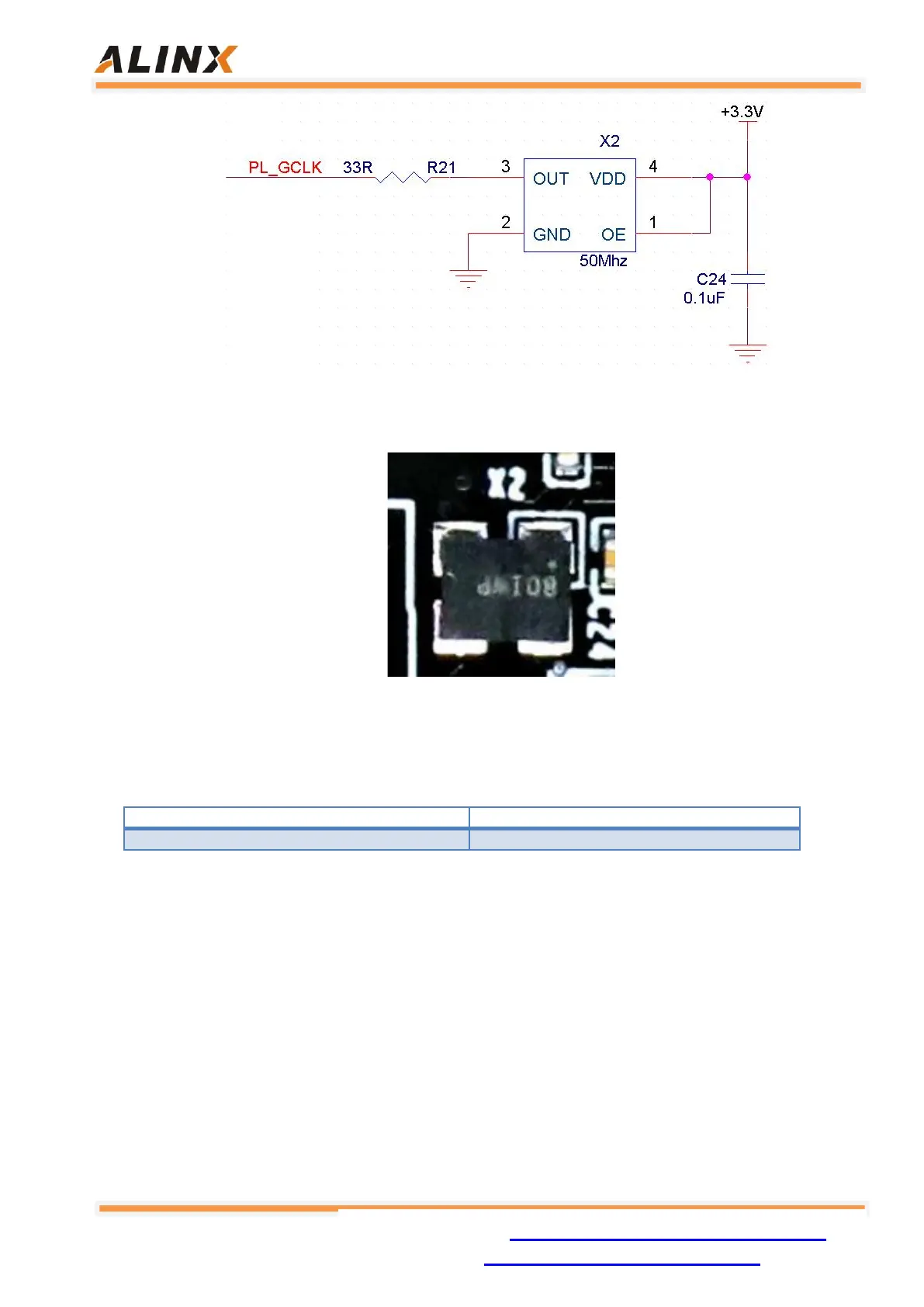
Figure 6-3: PL system clock source
Figure 6-4: 50 Mhz oscillator on the Core Board
PL Clock pin assignment:
Table 6-2: PL Clock pin assignment
GTP differential clock
The AC7015 core board provides a differential 125MHz GTP reference clock.
The differential LVDS clock output is connected to the reference clock of BANK112.
This 125Mhz clock can be used as the reference clock for fiber optic data
communication on the carrier board. The schematic diagram of the clock source is
shown in Figure 6-5