23 / 31
ZYNQ FPGA Development Platform AC7015 User Manual
Amazon Store: https://www.amazon.com/alinx
Sales Email: rachel.zhou@aithtech.com
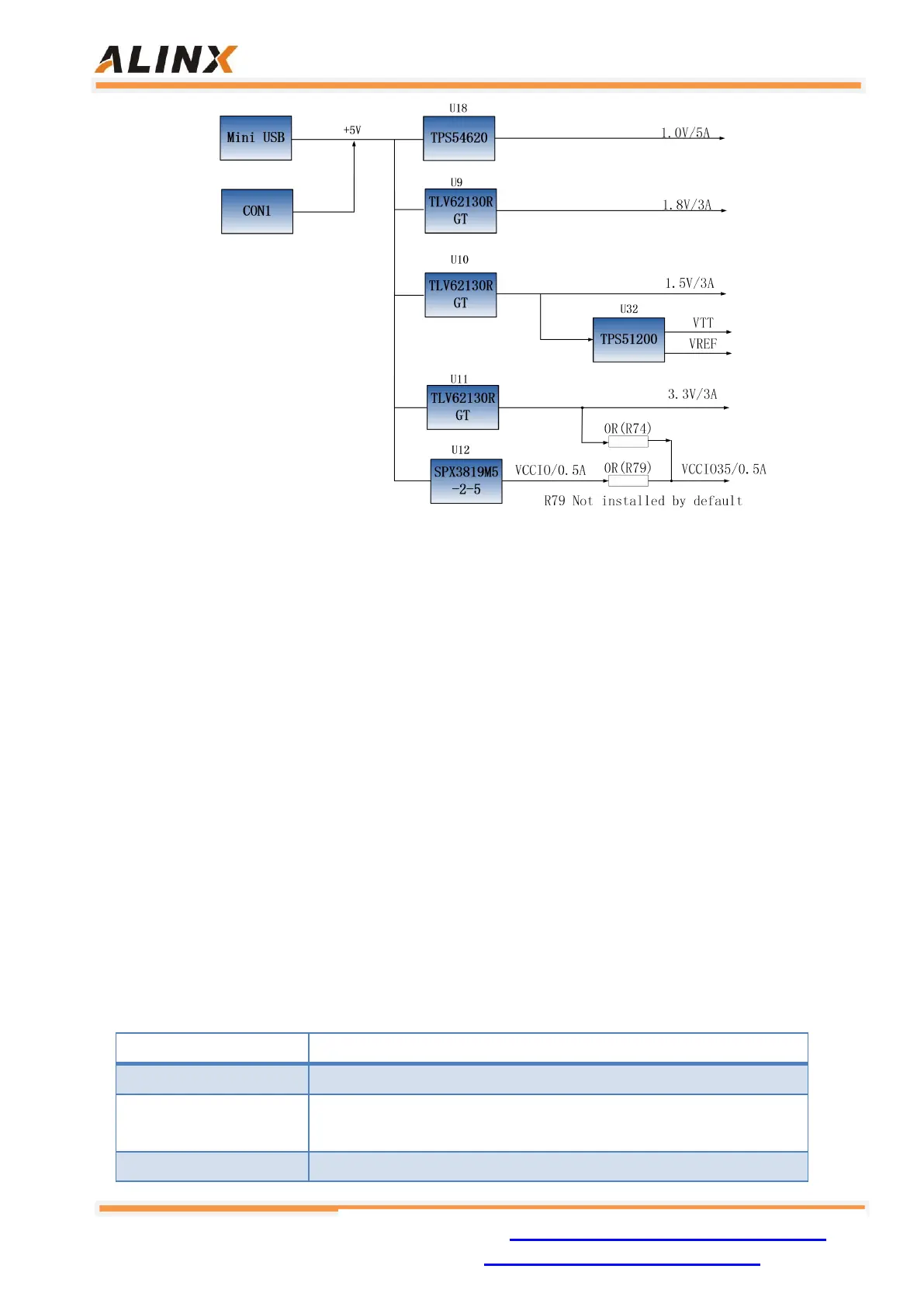
Figure 12-1: The Power Supply Design on the Core Board
The development board is powered by +5V, and is converted into +1.0V,
+1.8V, +1.5V, +3.3V four-way power supply through four-way DC/DC power supply
core TPS54620TLV62130RGT. The output current of +1.0V can be as high as 5A,
and the other three output current are 3A. The VCCIO 2.5V power supply is
generated by one LDO SPX3819M5-2-5. The VCCIO 2.5V power supply is mainly
reserved for the BANK power supply of the BANK35 of the FPGA. The user can
select the power supply of BANK35 through two 0 ohm resistors (R74, R79). By
default, the R74 on the development board is installed, and the resistor of R79 is
not installed, so the power supply of BANK35 is +3.3V. The user can replace the
resistor so that the IO of the BANK35 outputs a voltage standard of 2.5V. 1.5V
generates the VTT and VREF voltages required by DDR3 through TI's TPS51200.
The functions of each power distribution are shown in the following Table 12-1:
ZYNQ PS and PL section Core Voltage
ZYNQ PS and PL partial auxiliary voltage, BANK501 IO voltage,
eMMC
ZCNQ Bank0, Bank500, Bank13, Bank35 VCCIO, QSIP FLASH,