24 / 31
ZYNQ FPGA Development Platform AC7015 User Manual
Amazon Store: https://www.amazon.com/alinx
Sales Email: rachel.zhou@aithtech.com
Reserved for ZYNQ Bank33,Bank 34
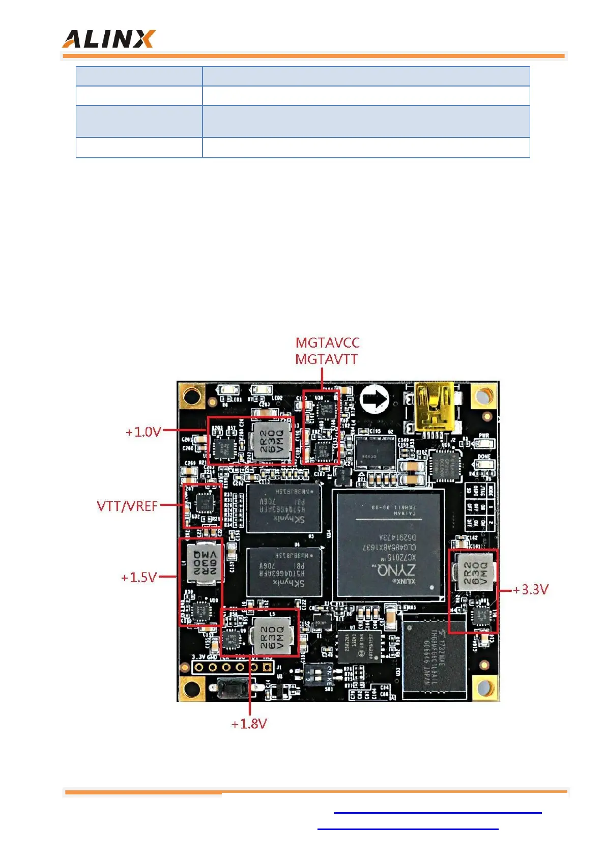
Table 12-1: The Functions of Each Power Distribution
Because the power supply of ZYNQ FPGA has the power-on sequence
requirement, in the circuit design, we have designed according to the power
requirements of the chip, and the power-on is +1.0V->+1.8V->(+1.5 V, +3.3V,
VCCIO). The circuit design ensures the normal operation of the chip. The power
supply on the core board detailed as Figure 12-2 below:
Figure 12-2: The Power Supply on the Core Board