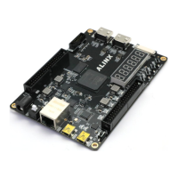
The ALINX ARTIX-7 FPGA Development Board AX7035 is a compact and versatile platform designed for FPGA development, featuring Xilinx's ARTIX-7 series FPGA chip (XC7A35T-2FGG484I, 484-pin FBGA package). The board measures 130mm x 90mm and is built on an 8-layer PCB, with four screw positioning holes (3.5mm diameter) for secure mounting.
Function Description:
The AX7035 board facilitates high-speed data processing and communication. It serves as a comprehensive development platform for various applications, including data buffering, network communication, image and video processing, and general-purpose FPGA logic development. Its extensive peripheral interfaces make it suitable for pre-verification and post-application in areas requiring high-speed data transmission, video processing, and industrial control. The board is designed to be a "Versatile" ARTIX-7 FPGA development platform, supporting students, engineers, and other groups engaged in FPGA development.
Important Technical Specifications:
FPGA Chip:
- Model: Xilinx ARTIX-7 series FPGA chip XC7A35T-2FGG484I (484-pin FBGA package).
- Logic Cells: 33,280
- Slices: 5,200
- CLB Flip-flops: 41,600
- Block RAM (kb): 1,800
- DSP Slices: 90
- Speed Grade: -2
- Temperature Grade: Industrial
Memory:
- DDR3 SDRAM: 2Gbit (256MB) high-speed DDR3 memory (Micron MT41J128M16HA-125, 128M x 16bit capacity). It serves as a buffer for FPGA chip data, with a 16-bit data bit width and a read/write clock frequency of up to 400MHz, providing a system bandwidth of up to 12.8Gb/s (800M*16bit).
- QSPI FLASH: 128Mbit QSPI FLASH (N25Q128) for storing FPGA configuration files and user data. It operates with a 3.3V CMOS voltage standard and can be used as a boot device.
- EEPROM: 24LC04 (4Kbit, 22568bit) for learning IIC bus communication.
Clock Source:
- Active Crystal Oscillator: 50MHz active crystal oscillator (Sitime) provides a stable system clock input to the FPGA (GCLK Pin Y18).
Power Supply:
- The board is powered by +5V and converts to +3.3V, +1.5V, +1.8V, +1.0V through a four DC/DC power supply chip TLV62130RGT. The output current can be up to 3A per channel. VCCIO is generated by one LDOSPX3819M5-3.3. VCCIO mainly supplies power to BANK16 of FPGA. Users can change the IO of BANK16 to different voltage standards by replacing the LDO chip. 1.5V generates the VTT and VREF voltages required by DDR3 via TI's TPS51200. In addition, 1.5V generates 1.2V to power the network interface chip through an LDO chip TPS74701.
- FPGA Power-up Sequence: VCCINT, then VCCBRAM, then VCCAUX, and finally VCCO. If VCCINT and VCCBRAM have the same voltage, they can be powered up simultaneously. The power-off sequence is reversed.
Interfaces:
- Gigabit Ethernet: 1-channel Gigabit Ethernet Interface (RJ-45) using Micrel's KSZ9031RNX Ethernet PHY chip, supporting 10/100/1000 Mbps network transmission rate (full duplex and adaptive). The transmission clock is 125MHz for Gigabit Ethernet and 25MHz for 100M Ethernet.
- HDMI Output: 1-channel HDMI image video output interface, supporting up to 1080P@60Hz output. It provides a +5V power supply to the HDMI display device when HDMI1_OUT_EN is high. Includes GTL2002D level conversion for IIC bus communication (FPGA 3.3V to HDMI 5V).
- HDMI Input/Output: 1-channel HDMI interface (J7) that can be used as both input and output. By default, it functions as an HDMI input, supporting up to 720P@60Hz input. It also includes GTL2002D level conversion for IIC bus communication.
- USB 2.0 Communication: 1-channel USB 2.0 Communication Interface using FTDI's FT232H single-channel high-speed USB chip, supporting 480Mb/s (high-speed) and 12Mb/s (full-speed) data communication. It supports various data communication modes (FIFO, I2C, SPI, JTAG) and reads external EEPROM configuration at power-on.
- USB to Serial Port: 1-channel USB-UART serial interface using Silicon Labs CP2102GM, connected via a MINI USB interface.
- SD Card Slot: 1-channel Micro SD slot, supporting SD mode and SPI mode.
- Expansion Headers: Two 40-pin (0.1-inch spacing) expansion headers (J9 and J10) for connecting ALINX modules or external circuits. Each header provides 1-channel 5V power supply, 2-channel 3.3V power supply, 3-channel ground, and 34 IOs. Warning: Do not directly connect the IO directly to the 5V device to avoid burning the FPGA. If you want to connect 5V equipment, you need to connect level conversion chip.
- FPC Expansion Ports: One 15-pin FPC expansion port (J8) for connecting a MIPI camera module. It supports 3 pairs of differential signals, 4 control signals, 1-channel 3.3V power supply (output), and 4-channel ground.
- JTAG Interface: 10-pin 0.1-inch spacing standard JTAG port for FPGA program download and debugging. Includes protection diodes to prevent damage from hot plugging.
Usage Features:
- Digital Tube Display: 6-digit, 8-segment digital tube for displaying digital information. It uses a common anode digital tube with dynamic display.
- User Keys: 1 reset key and 4 user keys (KEY1~KEY4) connected to the normal IO of the FPGA. Keys are active low.
- LED Lights: 7 red LEDs: 1 power indicator (PWR), 2 USB UART data receiving/sending indicators, and 4 user LEDs (LED1~LED4). User LEDs light up when the connected IO voltage is configured low and extinguish when configured high.
- Temperature Sensor: Onboard high-precision, low-power digital temperature sensor (LM75 of ON Semiconductor) with 0.5-degree accuracy. It connects to the FPGA via an I2C digital interface to read the board's ambient temperature.
Maintenance Features:
- Email Support: For corrections or errors in the English version of the manual, users can send an email to rachel.zhou@aithtech.com.
- Customer Service: Wechat/Skype: 15026866269. Technical Email: support@aithtech.com. Sales Email: rachel.zhou@aithtech.com.
- JTAG Hot Swapping: Users are advised to be careful not to hot swap when plugging and unplugging the JTAG cable to prevent damage.
- Expansion Header Protection: A 33 ohm resistor is included in series between the expansion port and the FPGA connection to protect the FPGA from external voltage or current.
- Power Supply Flexibility: The VCCO of BANK16 is powered by an LDO and can be changed by replacing the LDO chip, allowing for customization of voltage standards.