Amazon Store: https://www.amazon.com./alinx
Sales Email: rachel.zhou@aithtech.com
ARTIX-7 FPGA Development Board AX7035 User Manual
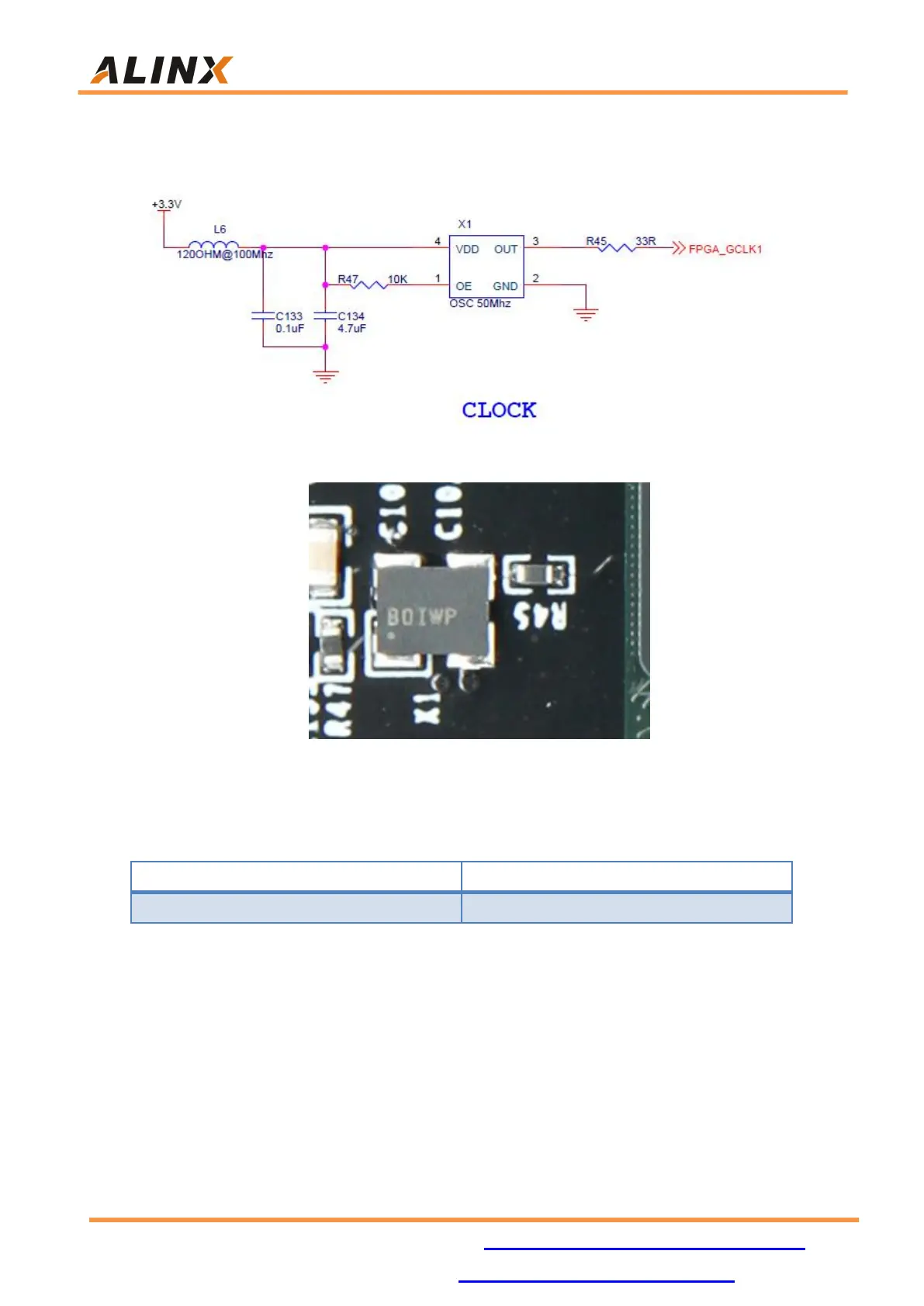
within the FPGA. The user can configure the FPGA's internal PLL and MMCM
to achieve a higher clock.
Figure 5-1: 50M active crystal oscillator
Figure 5-2: 50M active crystal oscillator on the FPGA Board
Clock Pin Assignment
Part 6:DDR3 DRAM
TheAX7035 FPGA development board is equipped with one Micron 2Gbit
(256MB) DDR3 chips, model MT41J128M16HA-125. DDR bus width is 16bit.
The DDR3 SDRAM has a maximum operating speed of 400MHz (data rate
800Mbps). The DDR3 memory system is directly connected to the memory