Amazon Store: https://www.amazon.com./alinx
Sales Email: rachel.zhou@aithtech.com
ARTIX-7 FPGA Development Board AX7035 User Manual
Part 11: USB 2.0 Communication Interface
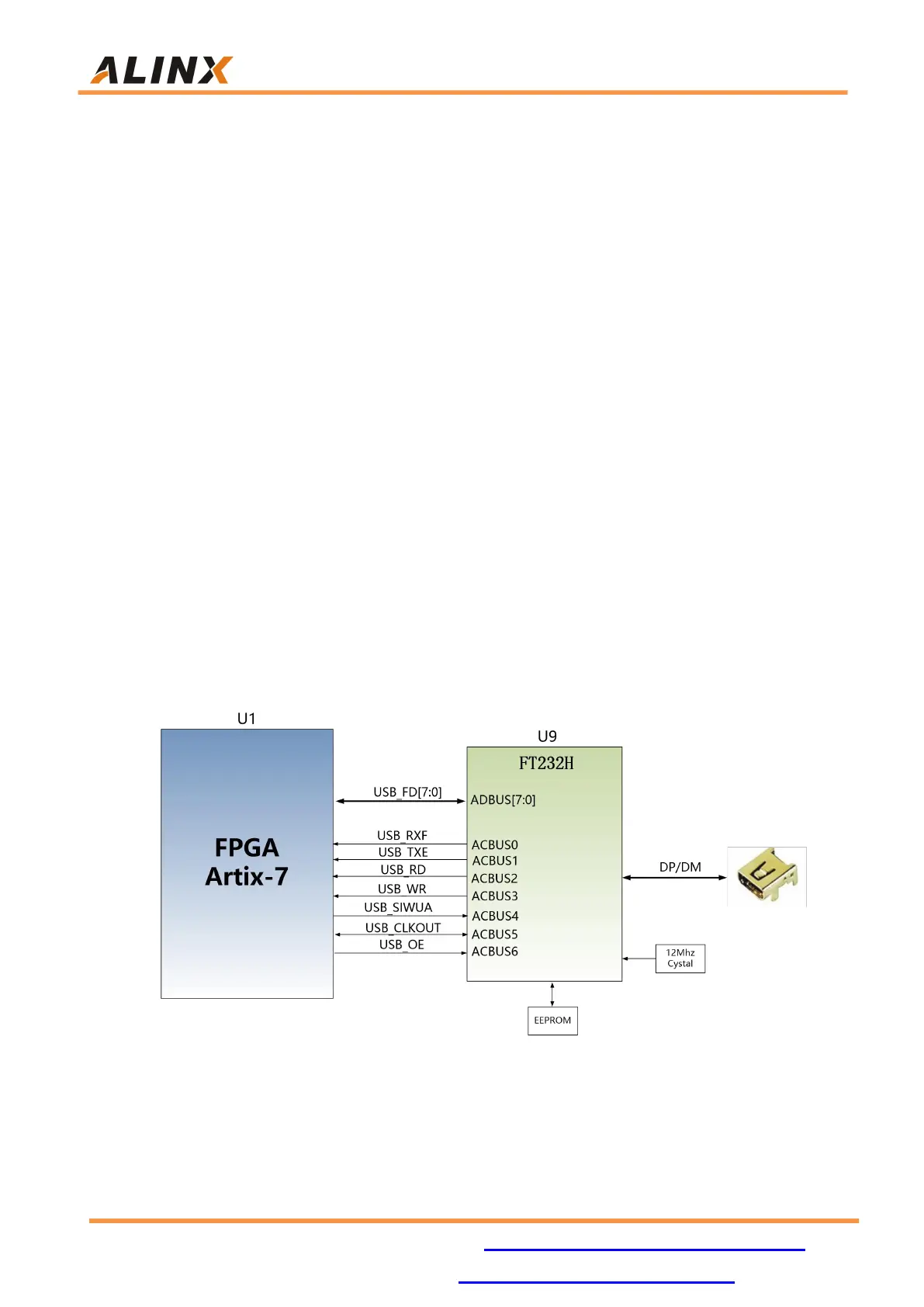
In the AX7035 FPGA development board, usedFT232H single-channel
high-speed USB chip of FEDI, to realize USB2.0 data communication between
the FPGA development board and the computer. Maximum USB2.0 high-speed
communication (480Mb/s) and full-speed communication (12Mb/s). The data
interface supports different data communication modes (FIFO, I2C, SPI, JTAG).
After power-on, read the external EEPROM configuration. Determining the
data communication mode, you can also easily modify the configuration mode
through the PC. The function of the interface pins of the USB chip is
multiplexed. For details, please refer to the FT232H chip manual.
The data interface signal of the USB chip FT232H is connected to the IO of
the FPGA. The data communication of the FT232H is performed by
programming of the FPGA. The hardware connection of the FT232H is
connected according to the FT245 synchronous FIFO interface. As shown in
Figure 11-1.
Figure 11-1: USB2.0 Interface schematic