Amazon Store: https://www.amazon.com./alinx
Sales Email: rachel.zhou@aithtech.com
ARTIX-7 FPGA Development Board AX7035 User Manual
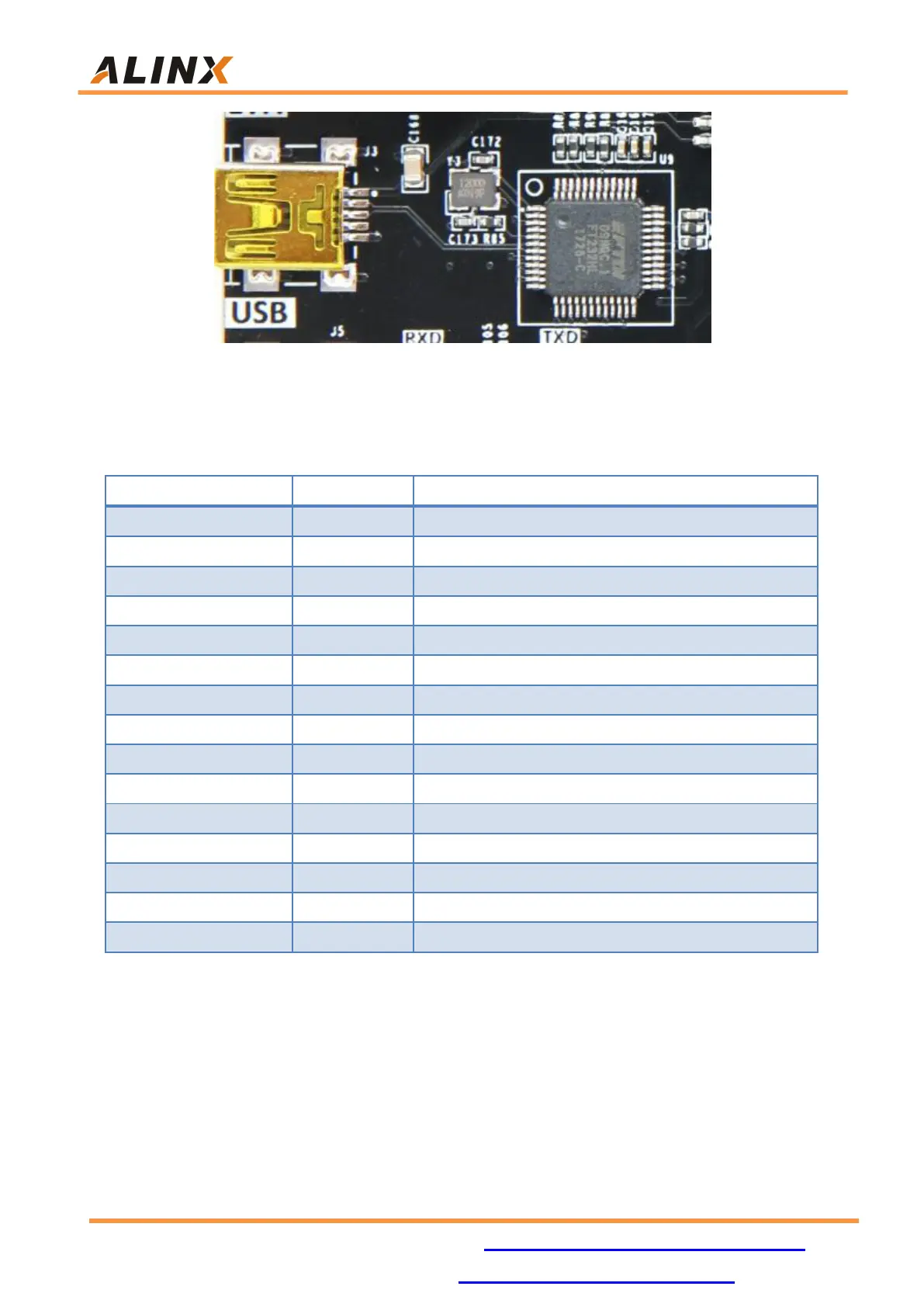
Figure 11-2: USB 2.0 part on the FPGA Board
USB 2.0 Pin Assignment
Low indicates that the receive FIFO data is readable
Low indicates that the send FIFO data can be written
Data receive FIFO read signal, low active
Data transmission FIFO write signal, low active
Send immediately/wake up function
Part 12: SD Card Slot
The SD card (Secure Digital Memory Card) is a memory card
based on the semiconductor flash memory process. It was
completed in 1999 by the Japanese Panasonic-led concept, and the
participants Toshiba and SanDisk of the United States conducted