Amazon Store: https://www.amazon.com./alinx
Sales Email: rachel.zhou@aithtech.com
ARTIX-7 FPGA Development Board AX7035 User Manual
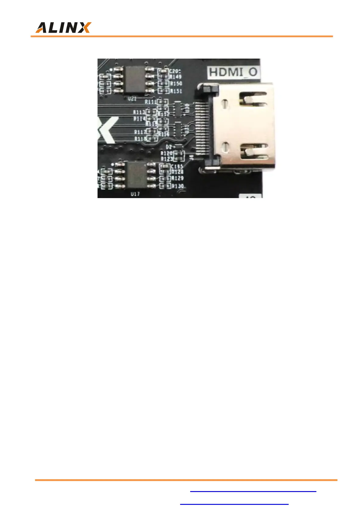
Figure 9-5: HDMI Input Interface on the FPGA Board
Part 10: HDMI1 input interface (also used as an
output)
The HDMI2 interface (J7) on the AX7035 development board can be used
as both an HDMI input and an HDMI output. By default, the HDMI2 interface is
used as an HDMI input. The data differential signal and clock signal of the
HDMI interface are directly connected to the differential IO of the FPGA. The
HMDI signal is transmitted in parallel and decoded in the FPGA to realize the
transmission solution of HDMI digital video input, and the function of up to
720P@60Hz input is supported.
The HDMI differential drive signal is passed through the IO input of the
FPGA BANK35, and the ESD protection device is added to the signal interface.
In addition, the HPD (hot plug detect) signal is output as the HDMI slave device,
and the high level indicates that the HDMI display slave device has been
inserted. Figure 10-1 shows the schematic of the HDMI input design.