Amazon Store: https://www.amazon.com./alinx
Sales Email: rachel.zhou@aithtech.com
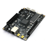
ARTIX-7 FPGA Development Board AX7035 User Manual
The main parameters of the FPGA chip XC7A35T are as follows
FPGA power supply system
Artix-7 FPGA power supplies are V
CCINT
, V
CCBRAM
, V
CCAUX
,V
CCO
, V
MGTAVCC
and
V
MGTAVTT
. V
CCINT
is the FPGA core power supply pin, which needs to be connected
to 1.0V; VCCBRAM is the power supply pin of FPGA block RAM, connect to 1.0V;
VCCAUX is FPGA auxiliary power supply pin, connect 1.8V; VCCO is the voltage of
each BANK of FPGA, including BANK0, BANK14~16, BANK34~35. On
AX7035 FPGA development board, BANK34 need to be connected to DDR3,
the voltage connection of BANK is 1.5V, and the voltage of other BANK is 3.3V.
The VCCO of BANK16 is powered by the LDO, and can be changed by replacing
the LDO chip. Because the GTP transceiver function is not used here, the
development board does not provide GTP power.
The Artix-7 FPGA system requires that the power-up sequence be
powered by VCCINT, then VCCBRAM, then VCCAUX and finally VCCO. If VCCINT and VCCBRAM
have the same voltage, they can be powered up at the same time. The order of
power outages is reversed.
Part 5: 50M active crystal oscillator
The Sitime 50M active crystal is provided on the development board to the
FPGA as the system clock input. The crystal output is connected to the FPGA's
global clock (GCLK Pin Y18). This GCLK can be used to drive the user logic