Amazon Store: https://www.amazon.com./alinx
Sales Email: rachel.zhou@aithtech.com
ARTIX-7 FPGA Development Board AX7035 User Manual
JTAG Interface
A 10-pin0.1 spacing standard JTAG ports for FPGA program download
and debugging.
Key
1 reset key, 4 user keys
LED Light
6LEDs, 1 power indicator, 1 DONE configuration indicator, 2 serial
transmit and receive indicators, 4 user LEDs.
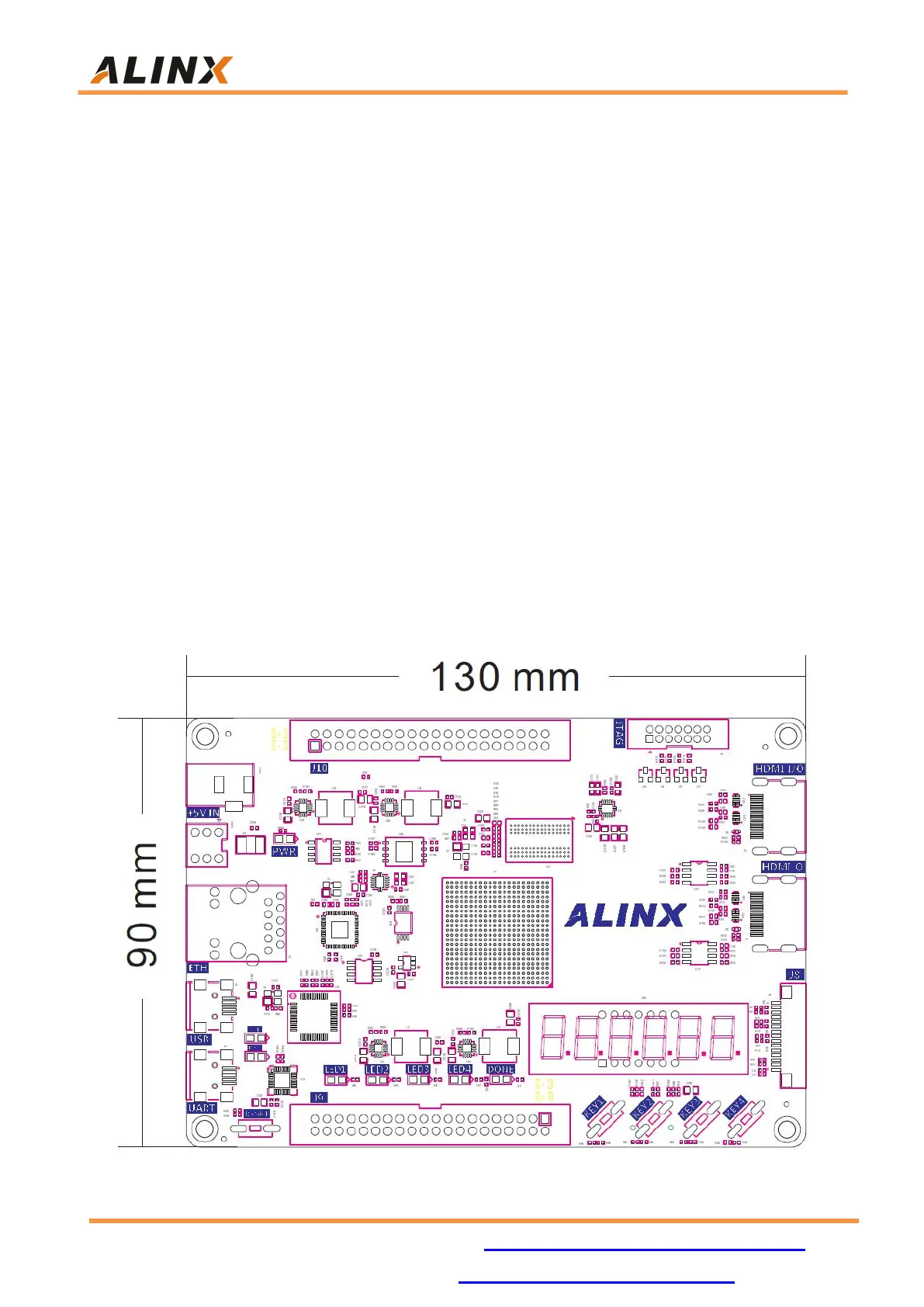
Part 2: Structure Diagram
The size of the development board is a compact 130mm x 90mm, and the
PCB is designed with an 8-layer board. There are 4 screw positioning holes
around the FPGA board for fixing the development board. The hole diameter of
the positioning hole is 3.5mm (diameter)
Figure 2-1: Structure Diagram