Amazon Store: https://www.amazon.com./alinx
Sales Email: rachel.zhou@aithtech.com
ARTIX-7 FPGA Development Board AX7035 User Manual
Part 8: Gigabit Ethernet Interface
The AX7035 development board provides network communication
services to users through a Micrel KSZ9031RNX Ethernet PHY chip. The
Ethernet PHY chip is connected to the IO interface of the ARTIX7 FPGA. The
KSZ9031RNX chip supports 10/100/1000 Mbps network transmission rate and
communicates with the FPGA through the RGMII interface. KSZ9031RNX
supports MDI/MDX adaptation, various speed adaptation, Master/Slave
adaptation, supports MDIO bus for PHY register management.
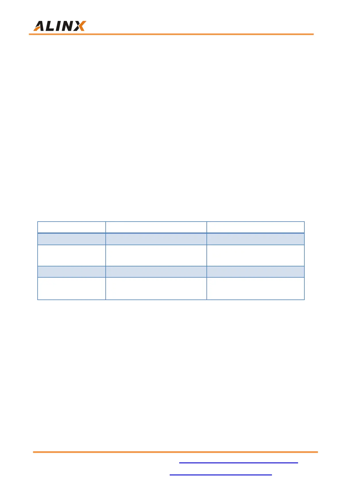
TheKSZ9031RNXwill detect the level status of some specific IOs to
determine their working mode after powered on. Table 8-1 describes the default
setup information after the GPHY chip is powered on.
MDIO/MDC Mode PHY Address
Enable 125Mhz clock output
selection
LED light mode configuration
Link adaptation and full duplex
configuration
10/100/1000 adaptive, compatible
with full-duplex, half-duplex
Table 8-1: PHY chip default configuration value
When the network is connected to Gigabit Ethernet, the data transmission
of FPGA and PHY chip KSZ9031RNXis communicated through the RGMII bus,
the transmission clock is 125Mhz, and the data is sampled on the rising and
falling of the clock.
When the network is connected to 100M Ethernet, the data transmission of
FPGA and PHY chip KSZ9031RNXis communicated through the RMII bus, the
transmission clock is 25Mhz,and the data is sampled on the rising and falling of
the clock.