Amazon Store: https://www.amazon.com./alinx
Sales Email: rachel.zhou@aithtech.com
ARTIX-7 FPGA Development Board AX7035 User Manual
Part 1: FPGA Development Board Introduction
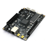
The AX7035 FPGA development board uses Xilinx's ARTIX-7 series of
FPGA chipsXC7A35T-2FGG484I, 484-pin FBGA package. The FPGA chip is
connected with a 256M byte DDR3 memory chip to achieve high-speed data
reading and writing between FPGA and DDR3. The data bit width is 16 bits, the
DDR read/write clock frequency reaches 400Mhz, and the bandwidth of the
whole system is up to 12.8Gb/s. (800M*16bit), which satisfies the data buffer
requirement during data processing. A 128Mbit QSPI FLASH is used as an
FPGA configuration chip to store FPGA configuration files and some user data.
The AX7035 FPGA development board has expanded a wide range of
peripheral interfaces, including one HDMI output interface, one HDMI input
interface, one Gigabit Ethernet interface, one USB2.0 interface, one UART
serial interface, one SD card interface, two 40-pin Expansion port, keys, LEDs,
EEPROM and sensor circuits.