Amazon Store: https://www.amazon.com./alinx
Sales Email: rachel.zhou@aithtech.com
ARTIX-7 FPGA Development Board AX7035 User Manual
Part 3: Power Supply
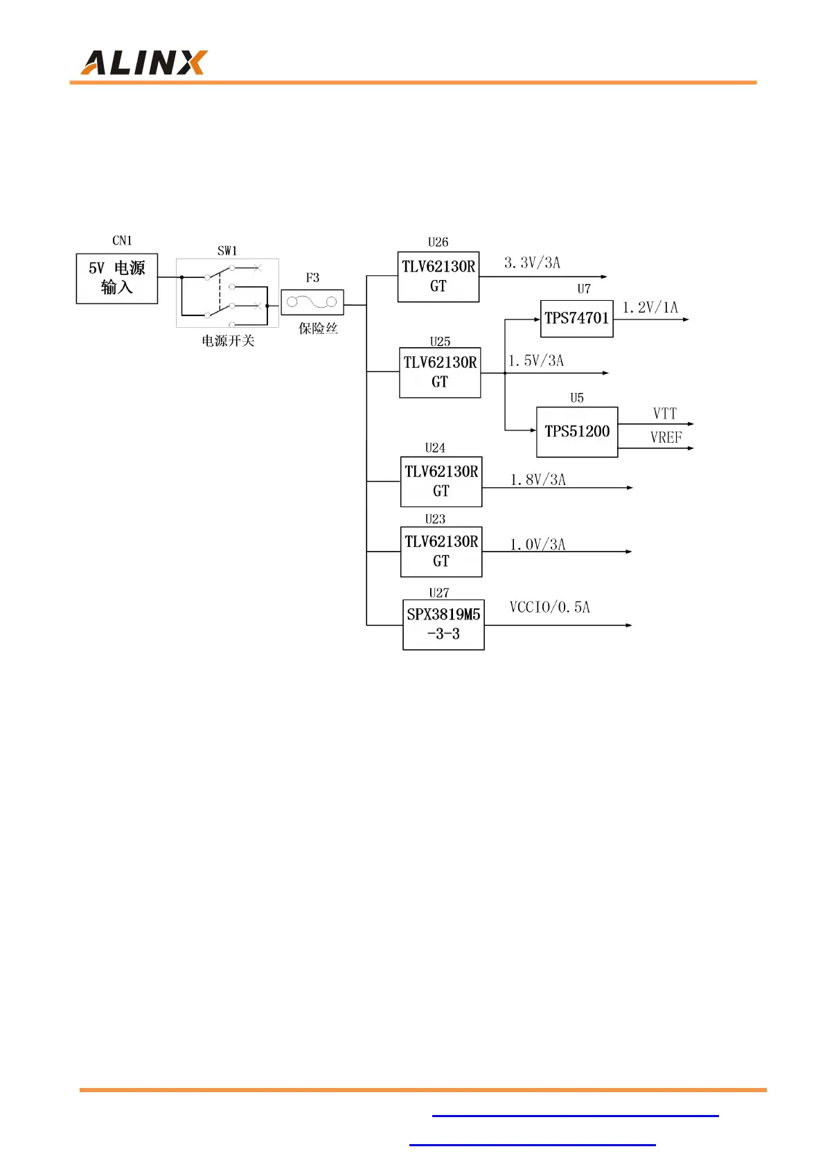
The power supply voltage of the AX7035 FPGA development board is
DC5V, and Figure 3-1 is the power supply schematic:
Figure 3-1: Power Supply Schematic
The development board is powered by +5V and converted to +3.3V, +1.5V,
+1.8V, +1.0V four-way power supply through four DC/DC power supply chip
TLV62130RGT. The output current can be up to 3A per channel. VCCIO is
generated by one LDOSPX3819M5-3-3. VCCIO mainly supplies power to
BANK16 of FPGA. Users can change the IO of BANK16 to different voltage
standards by replacing their LDO chip. 1.5V generates the VTT and VREF
voltages required by DDR3 via TI's TPS51200.In addition, 1.5V generates 1.2V
to power the network interface chip through an LDO chip TPS74701. The
functions of each power distribution are shown in the following table: