Amazon Store: https://www.amazon.com./alinx
Sales Email: rachel.zhou@aithtech.com
ARTIX-7 FPGA Development Board AX7035 User Manual
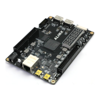
Figure 10-1: HDMI Input Interface Schematic
When the development board is used as an input device for HDMI display,
the power supply of HDMI1_5V is provided by the external main device. Here,
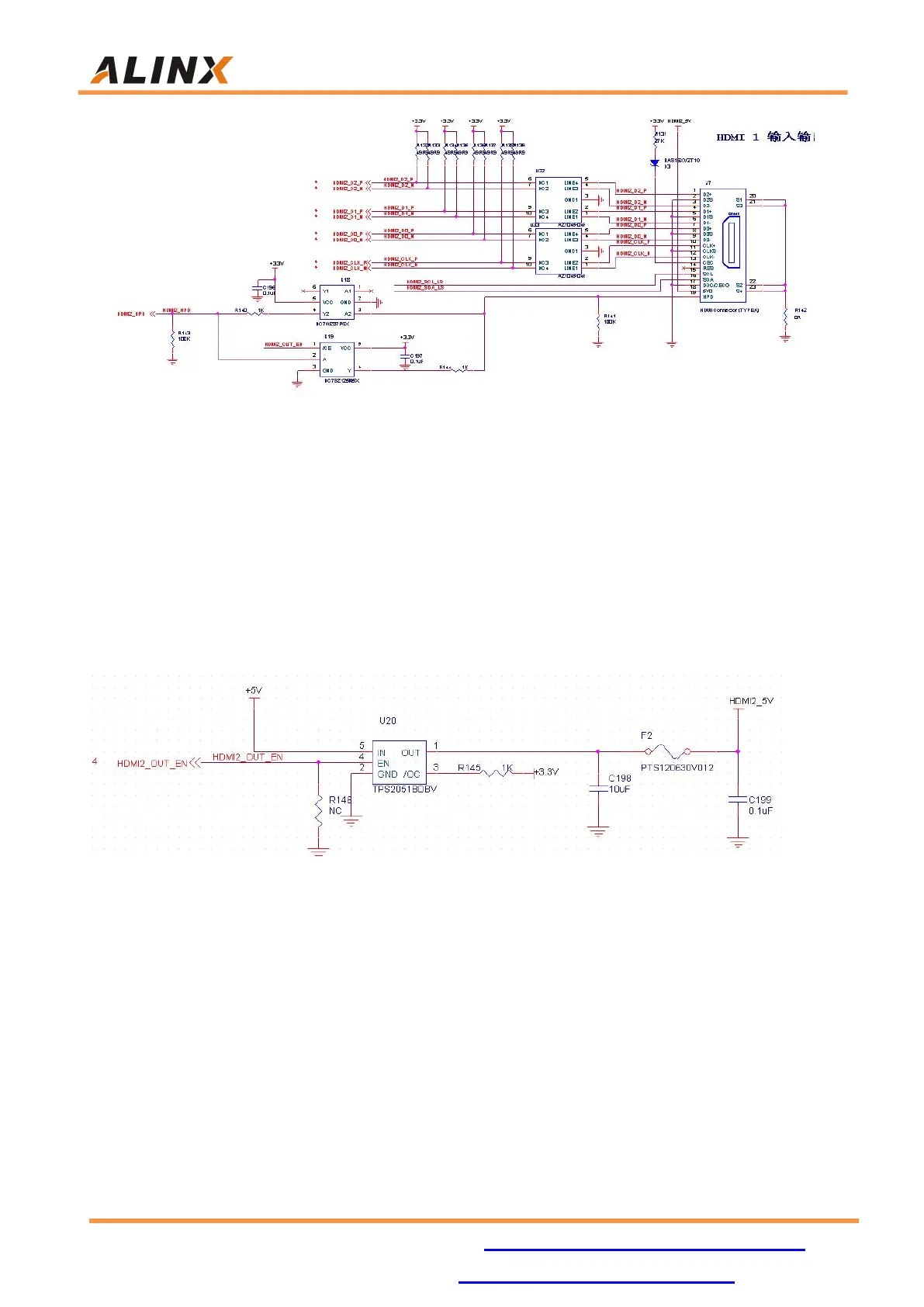
the signal of HDMI2_OUT_EN needs to be set to low level, and the output of
U20 chip is not enabled to be 5V. The HDMI2 power control circuit is shown in
Figure 10-2.
Figure 10-2: HDMI2 power control circuit
In addition, the HMDI master device reads the EDID device information of
the HDMI slave device through the IIC bus. The pin level of the FPGA is 3.3V,
but the level of HDMI is +5V. Here, the level conversion chip GTL2002D is
required to connect. The conversion circuit of IIC is shown in Figure 10-3.