Amazon Store: https://www.amazon.com./alinx
Sales Email: rachel.zhou@aithtech.com
ARTIX-7 FPGA Development Board AX7035 User Manual
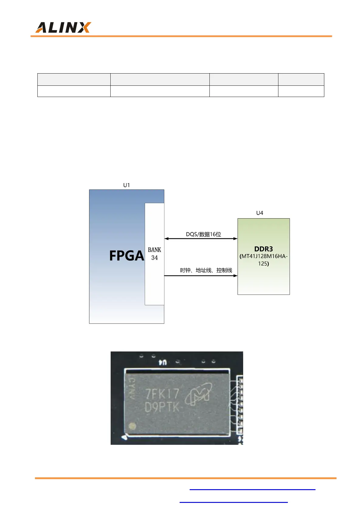
interface of the BANK 34 of the FPGA. The specific configuration of DDR3
SDRAM is shown in Table 6-1.
Table 6-1: DDR3 SDRAM Configuration
The hardware design of DDR3 requires strict consideration of signal
integrity. We have fully considered the matching resistor/terminal resistance,
trace impedance control, and trace length control in circuit design and PCB
design to ensure high-speed and stable operation of DDR3.
Figure 6-1: The DDR3 DRAM Schematic
Figure 6-2: The DDR3 on the FPGA Board