ADE9000 Technical Reference Manual UG-1098
Rev. 0 | Page 69 of 86
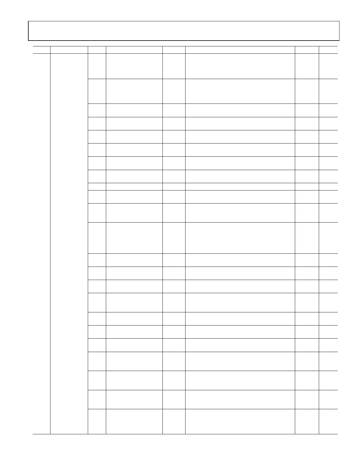
Addr. Name Bits Bit Name Settings Description Reset Access
This bit is set to indicate when the configuration
register CRC calculation is complete, after initiated
by writing the FORCE_CRC_UPDATE bit in the
CRC_FORCE register.
This bit is set if any of the registers monitored by
the configuration register CRC change value. The
CRC_RSLT register holds the new configuration
register CRC value.
25 DIPC This bit is set to indicates Phase C voltage
entered or exited a dip condition.
0x0 R/W1
24 DIPB This bit is set to indicates Phase B voltage
entered or exited a dip condition.
0x0 R/W1
23 DIPA This bit is set to indicates Phase A voltage
entered or exited a dip condition.
0x0 R/W1
22 SWELLC This bit is set to indicates Phase C voltage
entered or exited a swell condition.
0x0 R/W1
21 SWELLB This bit is set to indicates Phase B voltage
entered or exited a swell condition.
0x0 R/W1
20 SWELLA This bit it set to indicates Phase A voltage
entered or exited a swell condition.
0x0 R/W1
19 RESERVED Reserved. 0x0 R
This bit is set to indicate a phase sequence error
on the Phase voltage zero-crossings.
17 OI This bit is set to indicate that an overcurrent
event occurred on one of the phases indicated
in the OISTATUS register.
0x0 R/W1
16 RSTDONE This bit is set to indicate that the IC finished its
power-up sequence after a reset or after
changing between PSM3 operating mode to
PSM0, which indicates that the user can
configure the IC via the SPI port.
0x0 R/W1
15 ZXIC When this bit is set to 1, it indicates a zero-
crossing is detected on Phase C current.
0x0 R/W1
14 ZXIB When this bit is set to 1, it indicates a zero-
crossing is detected on Phase B current.
0x0 R/W1
13 ZXIA When this bit is set to 1, it indicates a zero-
crossing is detected on Phase A current.
0x0 R/W1
12 ZXCOMB When this bit is set, it indicates a zero-crossing is
detected on the combined signal from VA, VB,
and VC.
0x0 R/W1
11 ZXVC When this bit is set, it indicates a zero-crossing is
detected on the Phase C voltage channel.
0x0 R/W1
10 ZXVB When this bit is set, it indicates a zero-crossing is
detected on the Phase B voltage channel.
0x0 R/W1
9 ZXVA When this bit is set, it indicates a zero-crossing is
detected on the Phase A voltage channel.
0x0 R/W1
This bit is set to indicate a zero-crossing timeout
on Phase C. This means that a zero-crossing on
the Phase C voltage is missing.
7 ZXTOVB This bit is set to indicate a zero-crossing timeout
on Phase B. This means that a zero-crossing on
the Phase B voltage is missing.
0x0 R/W1
6 ZXTOVA This bit is set to indicate a zero-crossing timeout
on Phase A. This means that a zero-crossing on
the Phase A voltage is missing.
0x0 R/W1
5 VAFNOLOAD This bit is set when one or more phase
fundamental apparent energy enters or exits
the no load condition. The phase is indicated
in the PHNOLOAD register.
0x0 R/W1

 Loading...