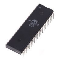
AT90S2313
25
•
Bit 6 - OCIE1A: Timer/Counter1 Output Compare Match Interrupt Enable
When the OCIE1A bit is set (one) and the I-bit in the Status Register is set (one), the Timer/Counter1 Compare Match inter-
rupt is enabled. The corresponding interrupt (at vector $004) is executed if a Compare match in Timer/Counter1 occurs,
i.e., when the OCF1A bit is set in the Timer/Counter Interrupt Flag Register - TIFR.
•
Bit 5,4 - Res: Reserved bits
These bits are reserved bits in the AT90S2313 and always read as zero.
•
Bit 3 - TICIE1: Timer/Counter1 Input Capture Interrupt Enable
When the TICIE1 bit is set (one) and the I-bit in the Status Register is set (one), the Timer/Counter1 Input Capture Event
Interrupt is enabled. The corresponding interrupt (at vector $003) is executed if a capture-triggering event occurs on
PD6(ICP), i.e., when the ICF1 bit is set in the Timer/Counter Interrupt Flag Register - TIFR.
•
Bit 2 - Res: Reserved bit
This bit is a reserved bit in the AT90S2313 and always reads as zero.
•
Bit 1 - TOIE0: Timer/Counter0 Overflow Interrupt Enable
When the TOIE0 bit is set (one) and the I-bit in the Status Register is set (one), the Timer/Counter0 Overflow interrupt is
enabled. The corresponding interrupt (at vector $006) is executed if an overflow in Timer/Counter0 occurs, i.e., when the
TOV0 bit is set in the Timer/Counter Interrupt Flag Register - TIFR.
•
Bit 0 - Res: Reserved bit
This bit is a reserved bit in the AT90S2313 and always read as zero.
Timer/Counter Interrupt FLAG Register - TIFR
•
Bit 7 - TOV1: Timer/Counter1 Overflow Flag
The TOV1 is set (one) when an overflow occurs in Timer/Counter1. TOV1 is cleared by hardware when executing the
corresponding interrupt handling vector. Alternatively, TOV1 is cleared by writing a logical one to the flag. When the I-bit in
SREG, and TOIE1 (Timer/Counter1 Overflow Interrupt Enable), and TOV1 are set (one), the Timer/Counter1 Overflow
Interrupt is executed. In PWM mode, this bit is set when Timer/Counter1 changes counting direction at $0000.
•
Bit 6 - OCF1A: Output Compare Flag 1A
The OCF1A bit is set (one) when compare match occurs between the Timer/Counter1 and the data in OCR1A - Output
Compare Register1 A. OCF1A is cleared by hardware when executing the corresponding interrupt handling vector. Alterna-
tively, OCF1A is cleared by writing a logical one to the flag. When the I-bit in SREG, and OCIE1A (Timer/Counter1
Compare match Interrupt Enable), and the OCF1A is set (one), the Timer/Counter1 Compare match Interrupt is executed.
•
Bits 5, 4 - Res: Reserved bits
These bits are reserved bits in the AT90S2313 and always read as zero.
•
Bit 3 - ICF1: - Input Capture Flag 1
The ICF1 bit is set (one) to flag an input capture event, indicating that the Timer/Counter1 value has been transferred to the
input capture register - ICR1. ICF1 is cleared by hardware when executing the corresponding interrupt handling vector.
Alternatively, ICF1 is cleared by writing a logical one to the flag. When the SREG I-bit, and TICIE1 (Timer/Counter1 Input
Capture Interrupt Enable), and ICF1 are set (one), the Timer/Counter1 Capture Interrupt is executed.
•
Bit 2 - Res: Reserved bit
This bit is a reserved bit in the AT90S2313 and always read as zero.
•
Bit 1 - TOV0: Timer/Counter0 Overflow Flag
The bit TOV0 is set (one) when an overflow occurs in Timer/Counter0. TOV0 is cleared by hardware when executing the
corresponding interrupt handling vector. Alternatively, TOV0 is cleared by writing a logical one to the flag. When the SREG
I-bit, and TOIE0 (Timer/Counter0 Overflow Interrupt Enable), and TOV0 are set (one), the Timer/Counter0 Overflow
interrupt is executed.
•
Bit 0 - Res: Reserved bit
This bit is a reserved bit in the AT90S2313 and always read as zero.
Bit 7 6 5 4 3 2 1 0
$38 ($58) TOV1 OCF1A - - ICF1 - TOV0 - TIFR
Read/Write R/W R/W R R R/W R R/W R
Initial value 0 0 0 0 0 0 0 0
 Loading...
