index
1.0 safety and servicing notes
1.1 Safety precautions ....................................................................................1
1.2 Electrostatic discharge precautions .............................................................1
1.3 Soldering.................................................................................................1
2.0 front and rear panel layouts
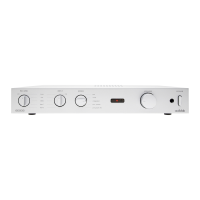
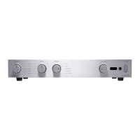
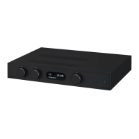
2.1 Front panel controls ..................................................................................3
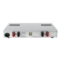
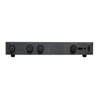
2.2 Rear panel connections .............................................................................3
3.0 disassembly instructionsPages 4 and 5 DELETED
4.0 functional tests
4.1 Test equipment required ............................................................................6
4.2 Functional test procedure...........................................................................7
5.0 performance tests
5.1 Test equipment required ..........................................................................11
5.2 Performance test procedure .....................................................................12
6.0 test points
6.1 Functional and performance test points .....................................................16
7.0 circuit schematics
7.1 Master schematic diagram (SCH267M-01-05)...........................................17
7.2 Line amplifier left channel schematic (SCH26701-07-02) ............................18
7.3 Line amplifier right channel schematic (SCH26701-08-02)..........................19
7.4 Power amplifier left channel schematic (SCH26701-09-02).........................20
7.5 Power amplifier right channel schematic (SCH26701-10-02).......................21
7.6 Power supplies schematic (SCH26701-01-02) ...........................................22
7.7 Protect and turn on schematic (SCH26701-06-02) .....................................23
7.8 Digital system controller schematic (SCH26701-02-01)...............................24
7.9 Digital system interface schematic (SCH26701-03-01)................................25
7.10 Input interface schematic (SCH26701-04-04) ............................................26
7.11 Relay coils schematic (SCH26701-05-01) .................................................27
7.12 Front panel schematic (SCH26702-01-01) ................................................28
7.13 Speaker outputs schematic (SCH26703-01-01)..........................................29
8.0 printed circuit board layout
8.1 Printed circuit board layout (top view).......................................................30
8.2 Printed circuit board layout (bottom view)..................................................31
9.0 technical data
9.1 8000S Technical specifications................................................................32
9.2 International standards............................................................................34