R911299720 / 02 | Rexroth IndraControl VCP 25 Electric Drives and Controls | Bosch Rexroth AG 10-1
List of Figures
10 List of Figures
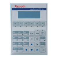
Fig. 1-1: VCP 25 with touch screen 1-1
Fig. 3-1: Hazard classification (according to ANSI Z535) 3-1
Fig. 5-1: Front panel dimensions 5-2
Fig. 5-2: Mounting cutout 5-3
Fig. 5-3: Side view and mounting depth for the standard device 5-4
Fig. 5-4: Side view and mounting depth for the field bus device 5-5
Fig. 6-1: Values for the representation type 6-1
Fig. 6-2: User mode switch 6-3
Fig. 7-1: Device variants 7-1
Fig. 7-2: Rear view of standard device 7-2
Fig. 7-3: 25 pin D-SUB female connector strip 7-4
Fig. 7-4: Pin assignment TTY / 20 mA, passive 7-4
Fig. 7-5: Pin assignment TTY / 20 mA, active 7-5
Fig. 7-6: 25 pin D-SUB female connector strip 7-6
Fig. 7-7: Pin assignment RS485 7-6
Fig. 7-8: Block diagram termination RS485 7-7
Fig. 7-9: Resistance values termination RS485 7-7
Fig. 7-10: Termination switch 7-7
Fig. 7-11: 25 pin D-SUB female connector strip 7-8
Fig. 7-12: Pin assignment RS232c 7-8
Fig. 7-13: 25-pin D-SUB female connector strip 7-9
Fig. 7-14: Pin assignment of the RS232c interface 7-9
Fig. 7-15: Rear view DeviceNet 7-10
Fig. 7-16: 9-pin D-SUB male and female connector strip 7-12
Fig. 7-17: Pin assignment DeviceNet 7-12
Fig. 7-18: Data line DeviceNet 7-12
Fig. 7-19: Baud rate DeviceNet 7-13
Fig. 7-20: Arrangement of the DeviceNet diagnostics LED 7-13
Fig. 7-21: Function of the DeviceNet diagnostics LED 7-13
Fig. 7-22: Rear view INTERBUS 7-14
Fig. 7-23: 9-pin D-SUB male and female connector strip 7-16
Fig. 7-24: Pin assignment INTERBUS 7-16
Fig. 7-25: Pin assignment INTERBUS 7-16
Fig. 7-26: Arrangement of the INTERBUS diagnostics LEDs 7-17
Fig. 7-27: Functions of the INTERBUS diagnostics LEDs 7-17
Fig. 7-28: Rear view PROFIBUS DP 7-18
Fig. 7-29: 9-pin D-SUB female connector strip 7-20
Fig. 7-30: Pin assignment PROFIBUS DP 7-20
Fig. 7-31: Baud rate PROFIBUS DP 7-21
Fig. 7-32: Arrangement of the PROFIBUS DP diagnostic LED 7-21
Fig. 7-33: Function of the PROFIBUS-DP diagnostic LED 7-21
Fig. 7-34: Rear view of the memory card 7-22
Fig. 7-35: Inserting the memory card 7-22
Fig. 7-36: Ejecting the memory card 7-23
Fig. 7-37: Shielding D-SUB connectors 7-23
Fig. 8-1: Nameplate (example) 8-2
Fig. 8-2: Pin assignment supply voltage 8-3
Fig. 8-3: Preparing the cable 8-4
Fig. 8-4: Connecting the female connector strip 8-4
Fig. 8-5: Female connector strip is plugged on 8-5
Fig. 8-6: Screws on the standard device (left) / field bus device

 Loading...