Copyright © 2021 congatec GmbH TCTLm02 60/67
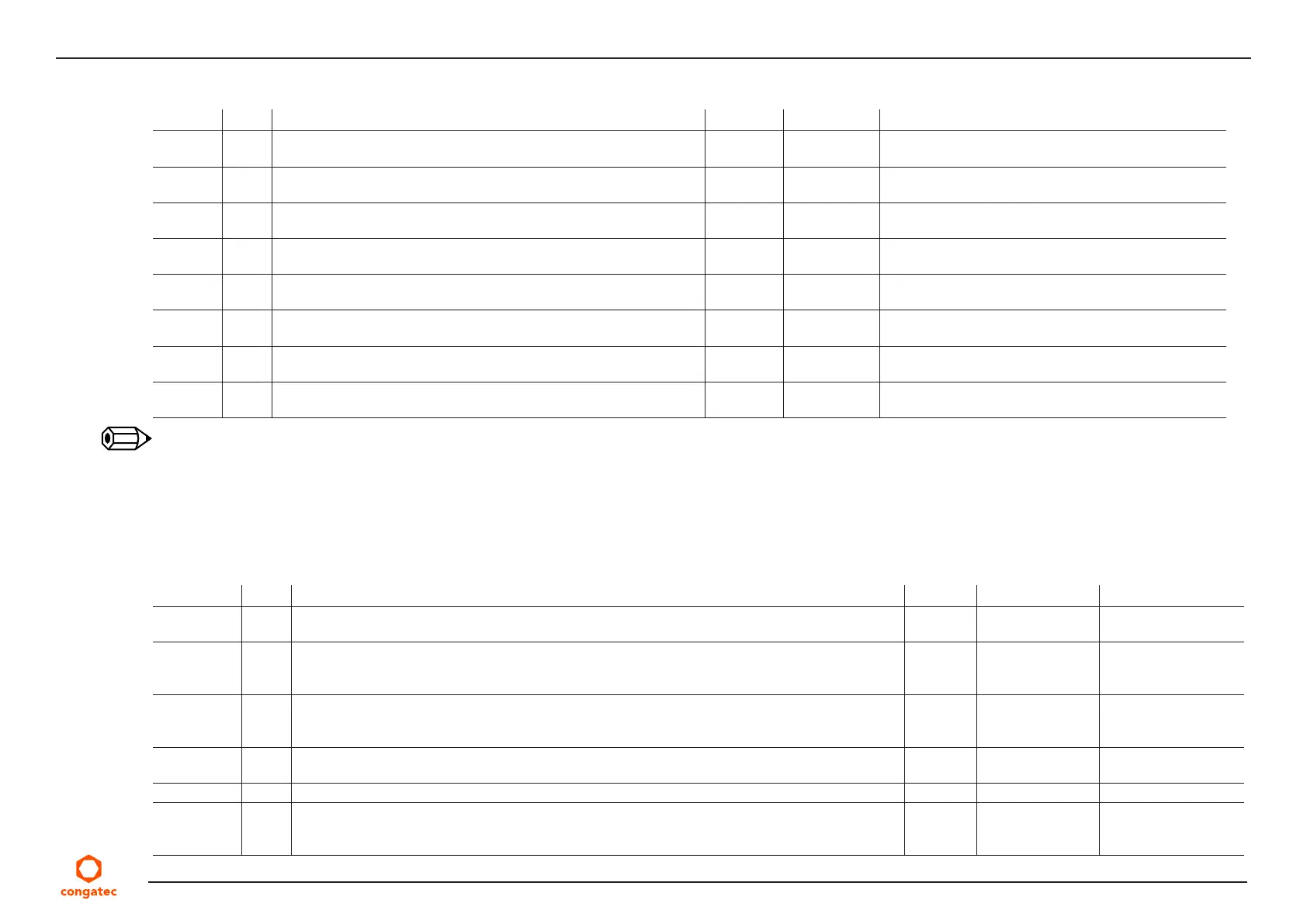
Table 31 General Purpose I/O Signal Descriptions
Signal Pin # Description I/O PU/PD Comment
GPO0 A93 General purpose output pins.
Shared with SD_CLK. Output from COM Express, input to SD
O 3.3 V
GPO1 B54 General purpose output pins.
Shared with SD_CMD. Output from COM Express, input to SD
O 3.3 V
GPO2 B57 General purpose output pins.
Shared with SD_WP. Output from COM Express, input to SD
O 3.3 V
GPO3 B63 General purpose output pins.
Shared with SD_CD. Output from COM Express, input to SD
O 3.3 V
GPI0 A54 General purpose input pins. Pulled high internally on the module.
Shared with SD_DATA0. Bidirectional signal
I 3.3 V PU 10KΩ 3.3 V
GPI1 A63 General purpose input pins. Pulled high internally on the module.
Shared with SD_DATA1. Bidirectional signal
I 3.3 V PU 10KΩ 3.3 V
GPI2 A67 General purpose input pins. Pulled high internally on the module.
Shared with SD_DATA2. Bidirectional signal
I 3.3 V PU 10KΩ 3.3 V
GPI3 A85 General purpose input pins. Pulled high internally on the module.
Shared with SD_DATA3. Bidirectional signal.
I 3.3 V PU 10KΩ 3.3 V
Note
The conga-TC570 provides GPIO signals on the COM Express connector by default.
Table 32 Power and System Management Signal Descriptions
Signal Pin # Description I/O PU/PD Comment
PWRBTN# B12 Power button to bring system out of S5 (soft off), active on falling edge.
Note: For proper detection, assert a pulse width of at least 16 ms
I 3.3 VSB PU 100 kΩ 3.3 VSB
SYS_RESET# B49 Reset button input. Active low input. Edge triggered. System will not be held in hardware reset
while this input is kept low.
Note: For proper detection, assert a pulse width of at least 16 ms.
I 3.3 VSB PU 10 kΩ 3.3 VSB
CB_RESET# B50 Reset output from module to Carrier Board. Active low. Issued by module chipset and may result
from a low SYS_RESET# input, a low PWR_OK input, a VCC_12V power input that falls below the
minimum specification, a watchdog timeout, or may be initiated by the module software.
O 3.3 V PD 100 kΩ
PWR_OK B24 Power OK from main power supply. A high value indicates that the power is good. I 3.3 V Set by resistor divider
to accept 3.3V
SUS_STAT# B18 Indicates imminent suspend operation; used to notify LPC devices. O 3.3 VSB
SUS_S3# A15 Indicates system is in Suspend to RAM state. Active-low output. An inverted copy of SUS_S3# on
the carrier board (also known as “PS_ON”) may be used to enable the non-standby power on a
typical ATX power supply.
O 3.3 VSB

 Loading...