8
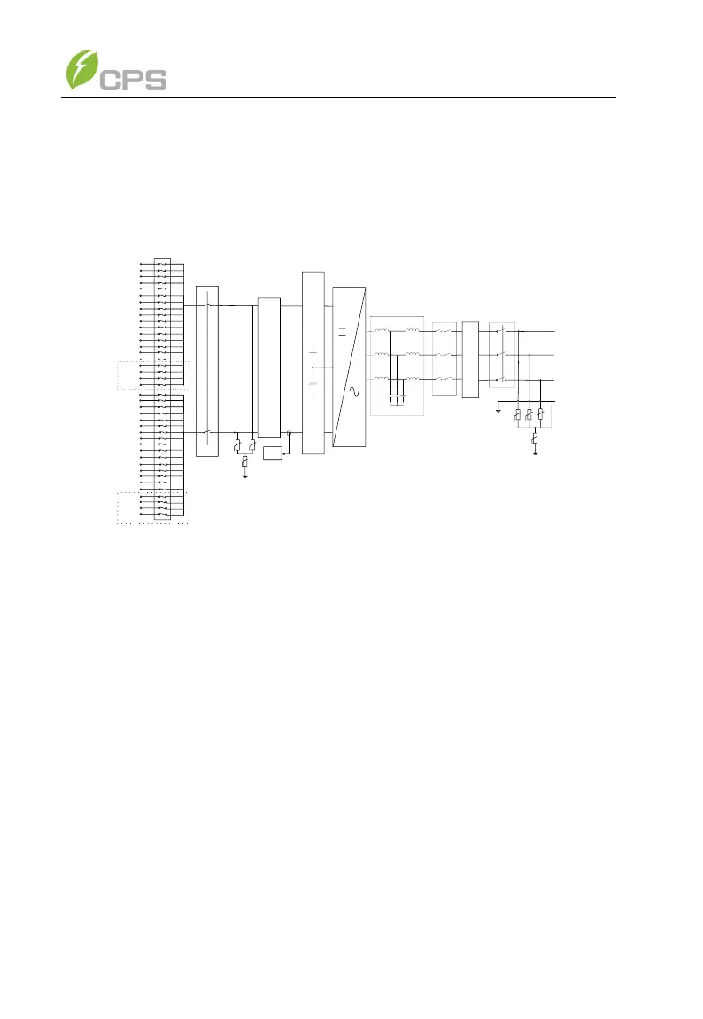
2.5 Schematic Diagram and Circuit Design
The basic electrical schematic diagram of CPS SCH100KTL-DO/US-600,
CPS SCH125KTL-DO/US-600 and CPS SCH100KTL-DO/US-480 inverters
are shown in Figure 2-2.
Figure 2-2 Schematic Diagram of the 100/125kW Inverter
The input from PV source circuits passes through surge protection circuitry,
DC EMI wave filter, to bus capacitance. The inverter then converts the DC
voltage to 3-phase AC voltage. Most of the high frequency AC harmonics are
removed with a wave filter. The output AC is connected to the grid via two-stage
relay. There is also a three-phase SPD at the AC output side.