User Guide DDOC0199-000-A9
1-Slot Data Transport System (CSfC) 3 - 2 Overview
© 2024 Curtiss-Wright Defense Solutions Revision 2.0
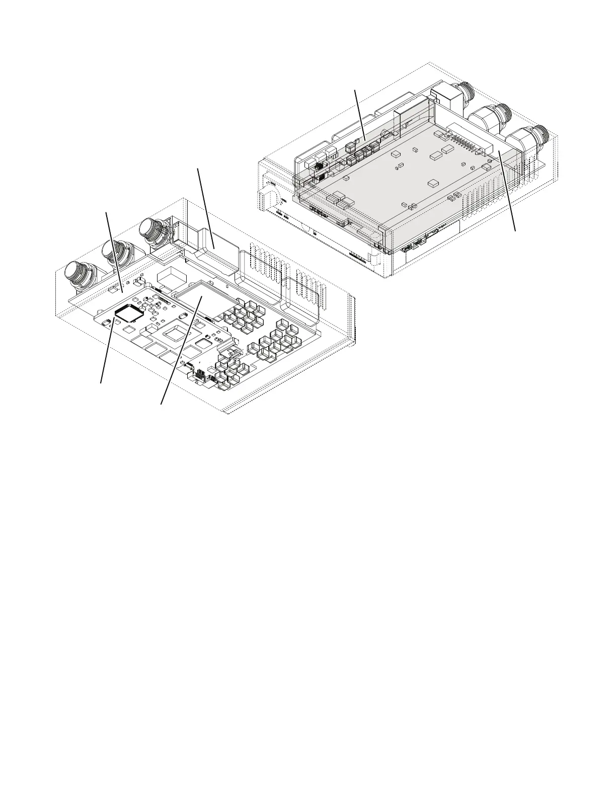
Figure 3.2 DTS1+ CSfC Chassis / Components
The RMC module mount positions the RMC module in the chassis. The backplane is used to
interface the RMC module to the processor carrier PCB. The mini comm PCB is the primary
assembly in the unit. It contains the processor / CPU, memory, and the encryption circuitry. The
processor carrier PCB is used to interface the mini comm PCB to the rest of the system. It also has
the utility (J2) and Ethernet (J3) connectors installed on it. The power supply assembly takes the
28 VDC input power, cleans and conditions it, and then distributes it to the entire system.
The enclosure is compliant with Military Specification MS25212 rail mounting standard for military/
aviation utilizing Dzus quarter-turn fasteners. A standard platform mounting option is also
available. Front panel LEDs give the user an at-a-glance DTS1+ CSfC status report. Additional
status information is available through the CLI.
Two rear panel 10/100/1000 Ethernet ports (connectors J2 and J3) (Figure 3.3) are available for
network connections supporting NFS, CIFS, FTP, iSCSI, PCAP, SFTP and HTTP file transfer
protocols. The DTS1+ CSfC also supports the Preboot eXecution Environment (PXE) giving
remote computers the capability to boot from files stored on the DTS1+ CSfC. Connector J2 also
supports RS-232 communication protocol (primarily used for configuring the DTS1+ CSfC) as well
as a discrete zeroize and reset function. Connector J1 is used to connect the DTS1+ CSfC to 28
VDC (operating voltage). In addition, the DTS1+ CSfC has a removable panel located on the
underside of the unit. It is removed to allow replacement of the crypto module battery.
A set of processor carrier PCB connections (Figure 3.4) is provided under a panel on the side of
the DTS1+ CSfC. Currently they are reserved for manufacturing and service activities. Contact
Curtiss-Wright for more information about end-user utilization of these connectors. A write-enable
switch is provided as well. The switch must be in the READ-WRITE position to enable configuring
the DTS1+ CSfC. Refer to paragraph 4.2.2 Write-Enable Switch for detailed information.
DDOC0199-0043
USB Flash
Module
COM Express
Module
Processor Carrier PCB
Power Supply PCB
RMC Module
Mount
Backplane
PCB