31
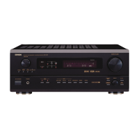
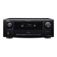
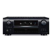
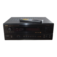
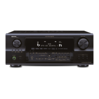
AVR-2807
PCM1803 (DI : IC301)
1
2
3
4
5
6
7
8
9
10
20
19
18
17
16
15
14
13
12
11
V
IN
L
V
IN
R
V
REF
1
V
REF
2
V
CC
AGND
PDWN
BYPAS
TEST
LRCK
MODE1
MODE0
FMT1
FMT0
OSR
SCKI
V
DD
DGND
DOUT
BCK
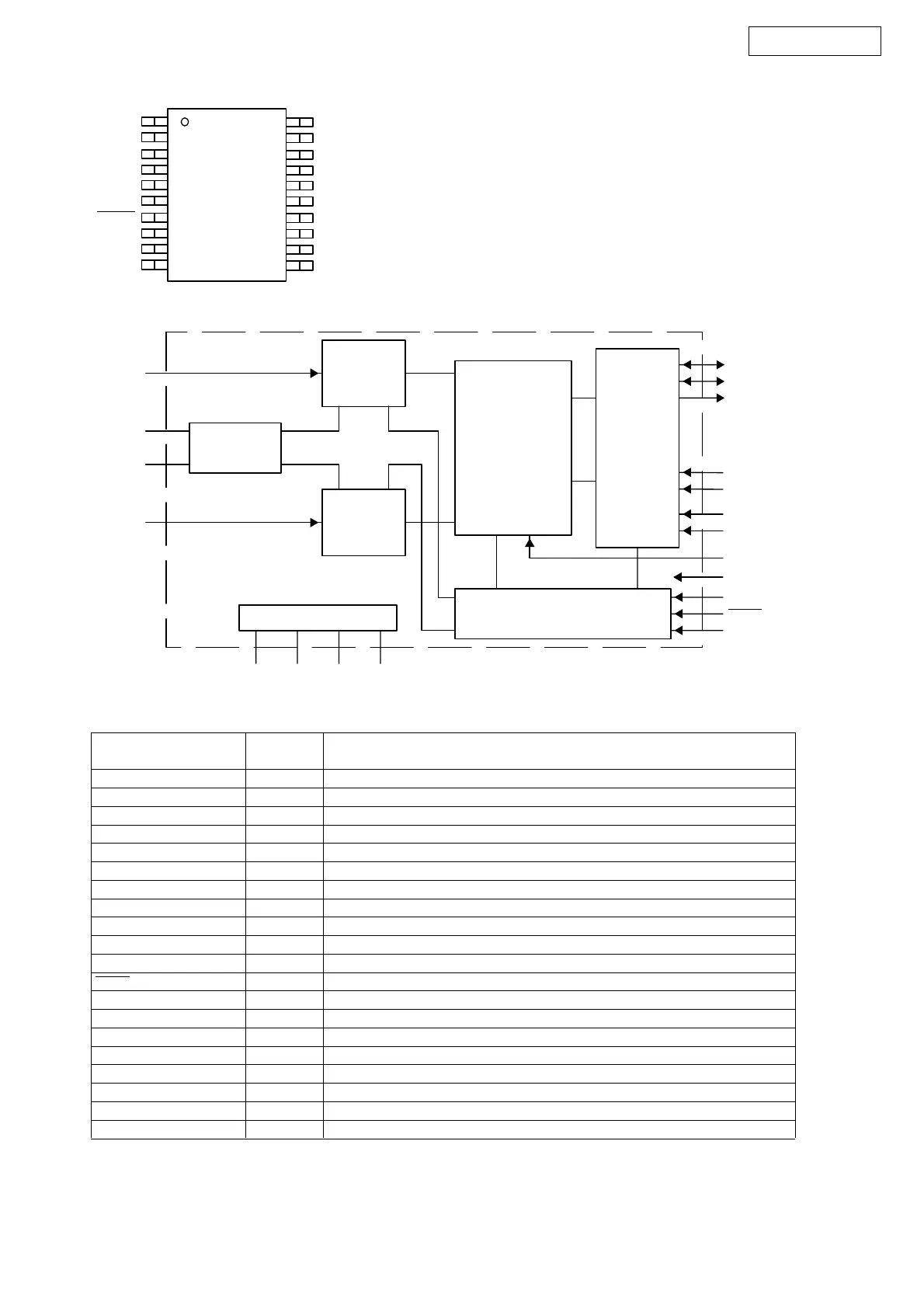
BLOCK DIAGRAM
BCK
V
IN
L
Reference
V
REF
1
V
REF
2
V
IN
R
DeltaœSigma
Modulator
DeltaœSigma
Modulator
x1/64 , x1/128
Decimation
Filter
With
HighœPass Filter
Power Supply
AGNDV
CC
V
DD
DGND
Clock and T iming Control
Serial
Interface
Mode/
Format
Control
LRCK
DOUT
FMT0
FMT1
MODE0
MODE1
BYPAS
OSR
PDWN
SCKI
TEST
TERMINAL FUNCTIONS
TERMINAL
I/O DESCRIPTION
NAME NO.
AGND 6 – Analog GND
BCK 11 I/O Audio data bit clock input/output
(1)
BYPAS 8 I HPF bypass control. LOW: Normal mode (dc reject); HIGH: Bypass mode (through)
(2)
DGND 13 – Digital GND
DOUT 12 O Audio data digital output
FMT0 17 I Audio data format select input 0. See Data Format section.
(2)
FMT1 18 I Audio data format select input 1. See Data Format section.
(2)
LRCK 10 I/O Audio data latch enable input/output
(1)
MODE0 19 I Mode select input 0. See Data Format section.
(2)
MODE1 20 I Mode select input 1. See Data Format section.
(2)
OSR 16 I Oversampling ratio select input. LOW: ×64 f
S
, HIGH: ×128 f
S
(2)
PDWN 7 I Power-down control, active-low
(2)
SCKI 15 I System clock input: 256 f
S
, 384 f
S
, 512 f
S
or 768 f
S
(3)
TEST 9 I Test, must be connected to DGND
(2)
V
CC
5 – Analog power supply, 5-V
V
DD
14 – Digital power supply, 3.3-V
V
IN
L 1 I Analog input, L-channel
V
IN
R 2 I Analog input, R-channel
V
REF
1 3 – Reference-voltage-1 decoupling capacitor
V
REF
2 4 – Reference-voltage-2 decoupling capacitor
(1) Schmitt-trigger input
(2) Schmitt-trigger input with internal pulldown (50 kΩ typically), 5-V tolerant
(3) Schmitt-trigger input, 5-V tolerant
 Loading...