33
DCD-1500AE
M66005-0001AHP (PD: IC603)
17
18
19
20
21
22
23
24
25
26
27
28
29
30
31
32
64
63
62
61
60
59
58
57
56
55
54
53
52
51
50
49
M66005-0001AHP
V
SEG33
SEG32
SEG31
SEG30
SEG29
SEG28
SEG27
SEG26
SEG25
SEG24
SEG23
SEG22
SEG21
SEG20
SEG19
SEG00
SEG01
SEG02
Vcc2
SEG39
SEG38
DIG13
DIG12
DIG09
DIG10
DIG11
DIG06
DIG07
DIG08
DIG04
DIG05
14
15
16
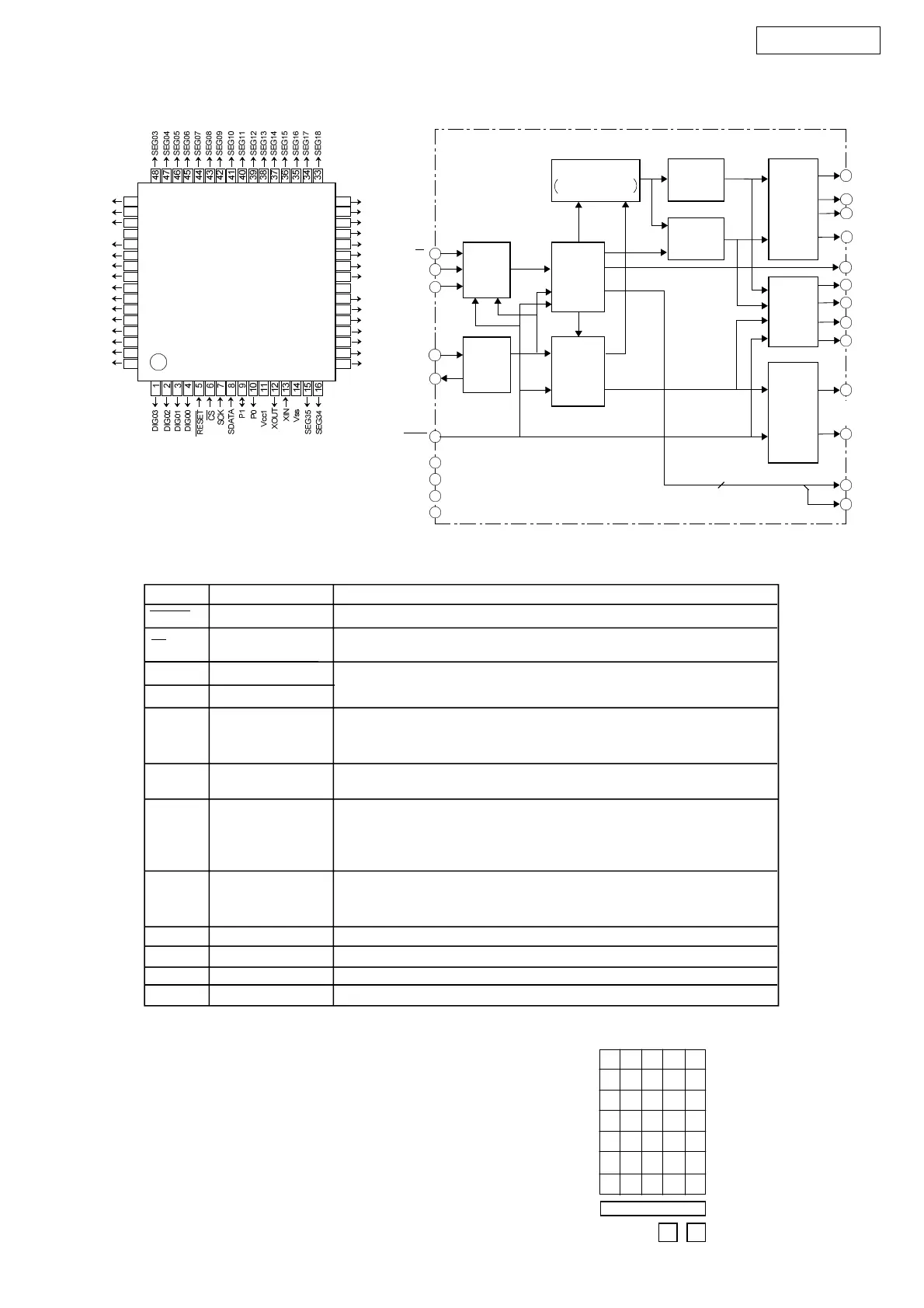
CGROM
(35bit x 160)
CGRAM
(35bit x 16)
code
write
data
dot data
write
code
select
timing
clock
59
33
31
24
64
63
62
61
DIG12
DIG13
SEG38
SEG39
SEG00
SEG26
.
.
.
SEG27
SEG34
.
.
.
.
.
.
.
.
.
12
1
DIG00
DIG11
.
.
.
.
.
.
scan
ulse
CS
SCK
SDATA
21
20
XIN
XOUT
13
RESET
BLOCK DIAGRAM
.
.
.
.
.
.
.
.
.
18
17
2
P0
P1
19
60
22
32
Vcc1
Vcc2
Vss
V
Serial
receive
circuit
Code/
command
control
circuit
Bank 1 : 8bit x 16
Bank 2 : 8bit x 64
Di sp l a y code RAM
Segment
output
circuit
Segment/
Digit
se l e c t /
output
circuit
Digit
output
circuit
Clock
generator
Di splay
controller
23
SEG35
..
.
.
.
.
.
.
.
.
RESET
SCK
SDATA
XIN ,
XOUT
P1, P0
Vcc1
Vcc2
Vss
Vp
Front view of VFD
PIN DESCRIPTIONS
Symbol
Pin name
Comment
Reset input
CS
Chip select input
When "L", M66005A is initialized.
When "L", communication with the MCU is possible.
When "H", any instruction from the MCU is neglected.
Shift clock input
Serial input data is taken and shifted by the positive edge of SCK.
Serial data input
Clock input
Clock output
When use as a CR oscillator, connect external resistor andcapacitor.
When use an external clock, input external clock to XIN, and XOUT
must be opened.
DIG00~
DIG15
Digit output
Connect to digit (grid) pins of VFD.
Connect to segment (anode) pins of VFD. Pins from SEG00 to SEG39
correspond to segment pins of VFD as shown in the table below.
SEG36~SEG39 pins are common to DIG12~DIG15 pins. So, when use
SEG36~SEG39, the number of digit to be used isdecreased.
Segment output
Universal port
Generally, use this port as the static output port.
This port also operateas s the timing IN/OUT port to control another
M66005A.
Positive power supply for internal logic.
Positive power supply for DIG and SEG outputs.
GND (0V)
Negative power supply to pull down.
( Connecti on of s e g ment output pins )
Each sq ua re sh ows on e-dot segm en t an d t he f ig ure in
the squ a re sho ws the output seg m e n t p i n n u m b e r
SEGnn (nn=00~39) to be connected.
SEG00~SEG34 are for character dot which are output
from character ROM or user RAM , an d SEG35~SEG39
are the dot which is controlled by command.
3433323130
2928272625
2423222120
1918171615
1413121110
0908070605
0403020100
35
3938
SEG00~
SEG39
P1 : bidirectional
P0 : output