41
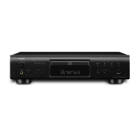
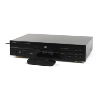
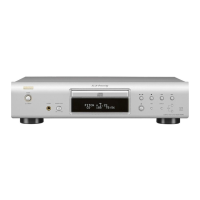
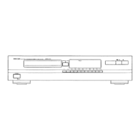
DCD-710AE
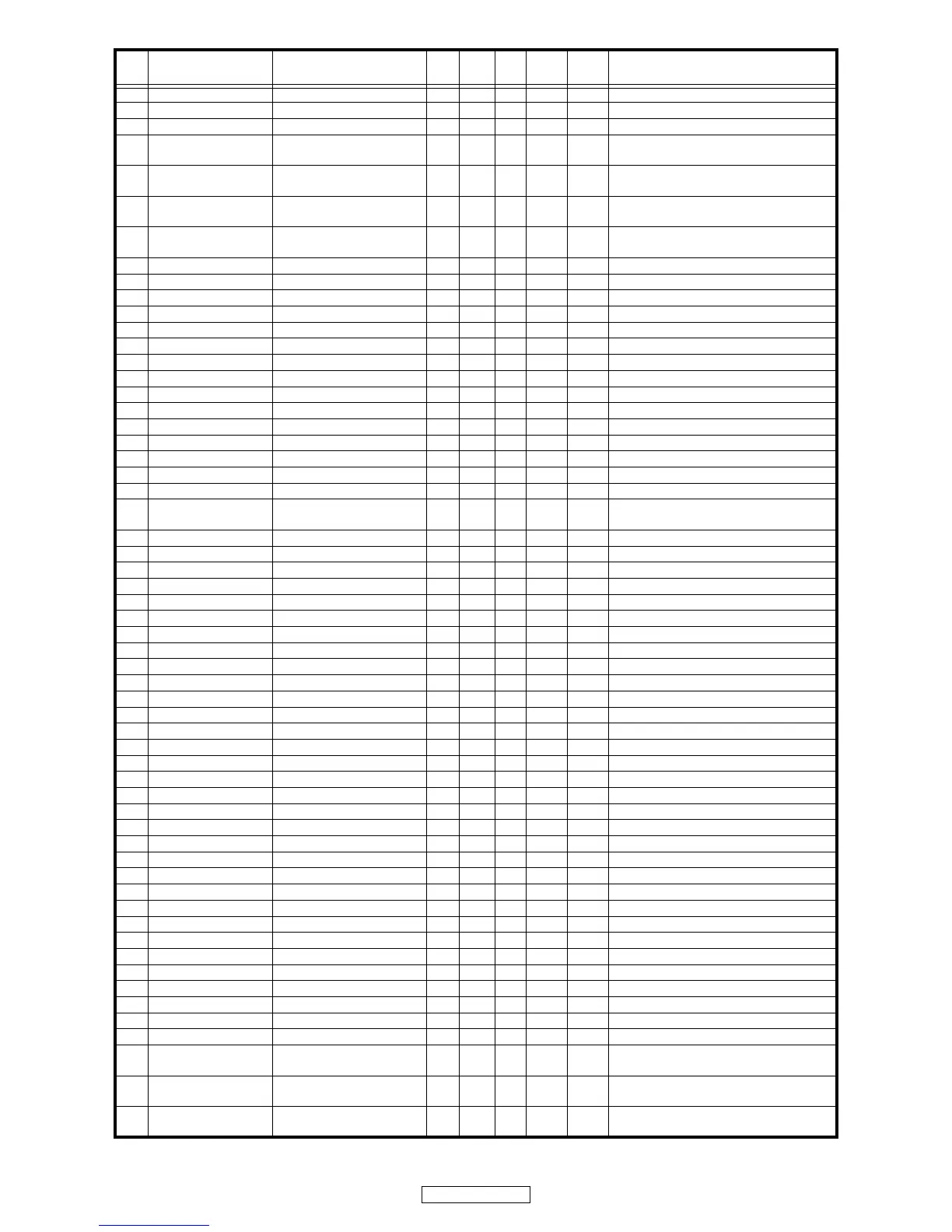
9 PWE Non (NC) O - O - - Output port
10 DVSS Power supply (GND) P P P P - Power supply (GND)
11 DVCC1B Power supply (+1.5V) P P P P - Power supply (+1.5V)
12 RVOUT1 Built-in +1.5V Regulator
output
O - O - - Voltage output is not in the Flash version
13 RVIN Built-in +1.5V Regulator
input
I - I - - Flash version is a terminal Power supply
14 RVIN Built-in +1.5V Regulator
input
I - I - - Flash version is a terminal Power supply
15 RVOUT2 Built-in +1.5V Regulator
output
O - O - - Voltage output is not in the Flash version
16 DVCC1A Power supply (+1.5V) P P P P - Power supply(+1.5V)
17 DVSS Power supply (GND) P P P P - Power supply(GND)
18 P00/D0 Non (NC) O - O(L) - - P0x : Setting is poss ble by 1bit unit
19 P01/D1 Non (NC) O - O(L) - - P0x : Setting is poss ble by 1bit unit
20 P02/D2 Non (NC) O - O(L) - - P0x : Setting is poss ble by 1bit unit
21 P03/D3 Non (NC) O - O(L) - - P0x : Setting is poss ble by 1bit unit
22 P04/D4 Non (NC) O - O(L) - - P0x : Setting is poss ble by 1bit unit
23 P05/D5 Non (NC) O - O(L) - - P0x : Setting is poss ble by 1bit unit
24 P06/D6 Non (NC) O - O(L) - - P0x : Setting is poss ble by 1bit unit
25 P07/D7 Non (NC) O - O(L) - - P0x : Setting is poss ble by 1bit unit
26 DVSS Power supply (GND) P P P P - Power supply (GND)
27 DVCC3A Power supply (+3.3V) P P P P - Power supply (+3.3V)
28 P10/D8 Non (NC) O - O(L) - PD P1x : Setting is poss ble by 1bit unit
29 P11/D9 Non (NC) O - O(L) - - P0x : Setting is poss ble by 1bit unit
30 P12/D10 Non (NC) O - O(L) - - P0x : Setting is poss ble by 1bit unit
31 P13/D11 MODEL ID L ; F107 H ;7
10AE
I - O(L) - - P0x : Setting is poss ble by 1bit unit
32 P14/D12 CHECK IN 100k PD O - O(L) - - P0x : Setting is poss ble by 1bit unit
33 P15/D13 CHECK 1 100k PD O - O(L) - - P0x : Setting is poss ble by 1bit unit
34 P16/D14 CHECK 2 100k PD O - O(L) - - P0x : Setting is poss ble by 1bit unit
35 P17/D15 CHECK 3 100k PD O - O(L) - - P0x : Setting is poss ble by 1bit unit
36 P40/A0 Non (NC) O - O(L) - - P4x : Setting is poss ble by 1bit unit
37 P41/A1 Non (NC) O - O(L) - - P4x : Setting is poss ble by 1bit unit
38 P42/A2 Non (NC) O - O(L) - - P4x : Setting is poss ble by 1bit unit
39 P43/A3 Non (NC) O - O(L) - - P4x : Setting is poss ble by 1bit unit
40 P44/A4 Non (NC) O - O(L) - - P4x : Setting is poss ble by 1bit unit
41 P45/A5 Non (NC) O - O(L) - - P4x : Setting is poss ble by 1bit unit
42 P46/A6 Non (NC) O - O(L) - - P4x : Setting is poss ble by 1bit unit
43 P47/A7 Non (NC) O - O(L) - - P4x : Setting is poss ble by 1bit unit
44 DVSS Power supply (GND) P P P P - Power supply (GND)
45 DVCC3A Power supply (+3.3V) P P P P - Power supply (+3.3V)
46 P50/A8 Non (NC) O - O(L) - - P5x : Setting is poss ble by 1bit unit
47 P51/A9 Non (NC) O - O(L) - - P5x : Setting is poss ble by 1bit unit
48 P52/A10 Non (NC) O - O(L) - - P5x : Setting is poss ble by 1bit unit
49 P53/A11 Non (NC) O - O(L) - - P5x : Setting is poss ble by 1bit unit
50 P54/A12 Non (NC) O - O(L) - - P5x : Setting is poss ble by 1bit unit
51 P55/A13 Reserved I - I - PU P5x : Setting is poss ble by 1bit unit
52 P56/A14 Reserved O - O(L) - PU P5x : Setting is poss ble by 1bit unit
53 P57/A15 Reserved I - I - PU P5x : Setting is poss ble by 1bit unit
54 P60/A16 Non (NC) O - O(L) - - P6x : Setting is poss ble by 1bit unit
55 P61/A17 Non (PD) O - O(L) - PD P6x : Setting is poss ble by 1bit unit
56 P62/A18 CCE O - I - PU P6x : Setting is poss ble by 1bit unit
57 P63/A19 BUCK O - I - PU P6x : Setting is poss ble by 1bit unit
58 P64/A20 BUS0 I/O - I - PU P6x : Setting is poss ble by 1bit unit
59 P65/A21 BUS1 I/O - I - PU P6x : Setting is poss ble by 1bit unit
60 P66/A22 BUS2 I/O - I - PU P6x : Setting is poss ble by 1bit unit
61 P67/A23 BUS3 I/O - I - PU P6x : Setting is poss ble by 1bit unit
62 DVSS Power supply (GND) P P P P - Power supply (GND)
63 DVCC3A Power supply (+3.3V) P P P P - Power supply (+3.3V)
64 P70/RD Non (NC) O - O(L) - - Port only for input
(Schmitt input and PU resistance)
65 P71/SRWR Non (NC) O - O(L) - - Port only for input
(Schmitt input and PU resistance)
66 P72/SRLLB Non (PD) O - O(L) - PD Port only for input
(Schmitt input and PU resistance)
Pin
No
IC Terminal name
DCD-710AE/755SE
Terminal name
I/O RST INIT STB
Pull
U/D
Port function