Do you have a question about the Denon DCD-710AE and is the answer not in the manual?
Service manual for the DENON DCD-710AE CD Player.
Procedure to check leakage current before returning unit.
Warning regarding laser beam exposure.
Important points to heed during servicing and inspection.
Step-by-step flow of the disassembly process.
Steps to disassemble the door.
Steps to disassemble the front panel assembly.
Steps to disassemble the CD mechanism assembly.
Procedure to remove the chucking plate.
Procedure to detach the CD tray.
Covers LD protection, handling, assembly, and defect checks.
How to enter and use service mode.
How to enter and use CD test mode.
Details of servo check, pickup control, stop, and all servos on procedures.
How to display laser current.
How to display adjustment values.
How to display accumulated laser on time.
Procedures for CD heat run modes.
Steps for normal heat run mode.
Steps for heat run short mode.
Steps for automatic mounting mode.
How to display and interpret errors.
How to perform firmware version up for main MCU.
How to initialize the unit.
How to perform firmware version up for USB MCU.
How to perform EEPROM test.
Steps for updating IC15 firmware.
Selecting the setup file in the programmer.
Navigating to the device selection tab.
Selecting the correct device and series.
Accessing the password setting.
Setting the device to blank state.
Navigating to the object file selection tab.
Opening the file browser.
Selecting the correct file format.
Indicating the file's location.
Accessing option settings.
Setting the erase option.
Navigating to communication settings.
Setting COM port and clock.
Powering on and resetting the target device.
Dialog box for data erase confirmation.
Initiating the writing process.
Troubleshooting steps for power issues.
Troubleshooting steps for blown fuses.
Troubleshooting steps for voltage output problems.
Troubleshooting steps for display problems.
Troubleshooting steps for +42V output.
Troubleshooting steps for key input problems.
Troubleshooting remote control issues.
Troubleshooting disc tray operation.
Troubleshooting audio output problems.
Component and foil layouts of the main PCB.
RF waveforms during disc playback.
Waveforms for disc detection.
Waveforms for TOC read.
Waveforms for focus adjustment.
Waveforms for loader operation.
Pin diagram for IC11.
Detailed pin functions for IC11.
More pin functions for IC11.
Pin diagram for IC15.
Block diagram of IC15.
Pin functions for IC15.
Terminal names and functions for IC15.
More terminal names and functions for IC15.
Pin diagram for IC17.
Terminal functions for IC17.
More terminal functions for IC17.
More terminal functions for IC17.
More terminal functions for IC17.
Pin diagram and block diagram for IC14.
Pin diagram and block diagram for IC36.
Pin connections for the FL display.
Grid assignments for the FL display.
Explanation of resistor part numbering and characteristics.
Explanation of capacitor part numbering and characteristics.
List of semiconductor parts.
List of resistor parts.
List of capacitor parts.
More capacitor parts.
More capacitor parts.
List of other miscellaneous parts.
More miscellaneous parts.
Semiconductors on the main PCB.
Capacitors on the main PCB.
More capacitors on the main PCB.
Other parts on the main PCB.
Parts list for the audio/power PCB.
List of screws used in the unit.
| Audio system | stereo |
|---|---|
| Audio formats supported | MP3, WMA |
| Signal-to-Noise Ratio (SNR) | 110 dB |
| Total Harmonic Distortion (THD) | 0.0025 % |
| CD-RW playback | Yes |
| Playback disc formats | CD audio |
| CD changer | No |
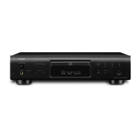
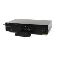
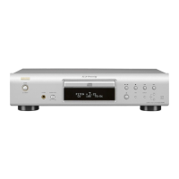
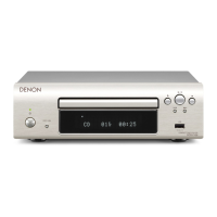
| Device type | HiFi CD player |
| Product color | Silver |
| Disc playback modes | Programming |
| Number of optical discs | 1 discs |
| Display type | VFD |
| Volume control | Digital |
| Programmable tracks | 25 |
| Headphone connectivity | 6.3 mm |
| USB 2.0 ports quantity | 1 |
| Power requirements | 230V AC, 50Hz |
| Power consumption (typical) | 22 W |
| Depth | 279 mm |
|---|---|
| Width | 434 mm |
| Height | 107 mm |
| Weight | 4200 g |