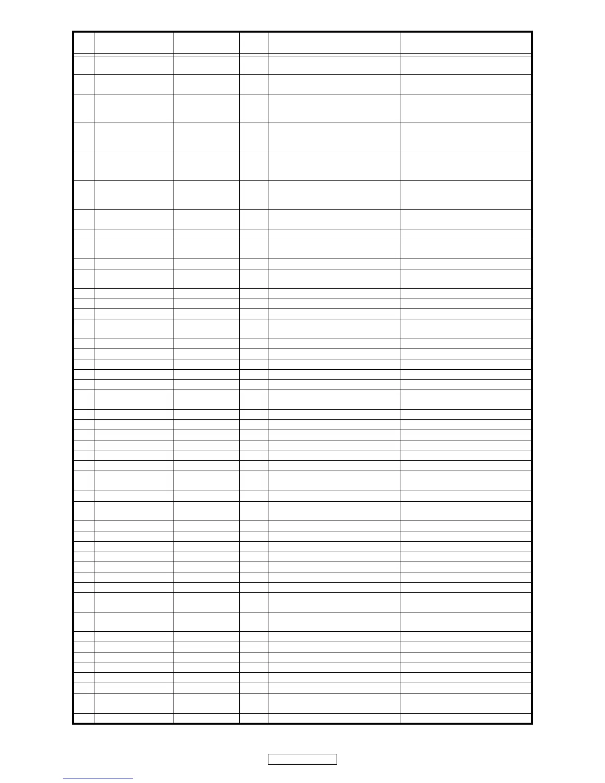
37
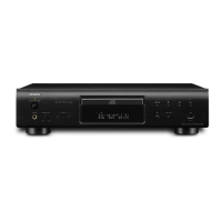
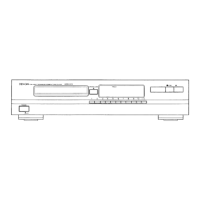
DCD-710AE
12 PF5/SCLK1/CTS1/
HSCLK
100K
Ω
/PD
I DENON BUS(F107 only) (Schmitt I input)
13 PN0/SCK0 CONT1 O Reserved (Schmitt I input), When resetting it, it
becomes output latch 1.
14 PN1/SO0/SDA0 CONT2 I Reserved (Schmitt I input and open drain output),
When resetting it, it becomes output
latch 1.
15 PN2/SI0/SCL0 CONT3 O Reserved (Schmitt I input and open drain output),
When resetting it, it becomes output
latch 1.
16 PN4/SO1/SDA1 E2P_DI O Cereal data output for E2PROM (Schmitt I input and open drain output),
When resetting it, it becomes output
latch 1.
17 PN5/SI1/SCL1 E2P_DO I Cereal data input for E2PROM (Schmitt I input and open drain output),
When resetting it, it becomes output
latch 1.
18 PN3/SCK1 E2P_CLK O Serial clock output for E2PROM (Schmitt I input)§When resetting it, it
becomes output latch 1.
19 PD0/TB0OUT0/INT4 PU I DENON BUS (F107 only) (Schmitt I input)
20 DVSS Power supply
(GND)
P Power supply (GND)
21 P74/INT0 REMOCON I Remote control input (710only) Port only for input (Schmitt)
22 DVCC Power supply
(+3.3V)
P Power supply(+3.3V)
23 P00/D0 OPEN_F O Tray OPEN control P0x : Setting is possible by 1bit unit
24 P01/D1 CLSE_F O Tray CLOSE control
25 P02/D2 A_Mute O DAC output audio mute L; Mute, H; Mute cancel
26 P03/D3 DRVMUTE O CD drive mute output L; Mute, H; Mute cancel (Cancels
above 3V)
27 P04/D4 INSW I CD drive limit SW input
28 P05/D5 CLSW I CD drive close SW input
29 P06/D6 OPSW I CD drive opening SW input
30 P07/D7 (USB_DET) PU I Reserved
31 P10/D8 FL_RST O FL tube communication line (reset) P1x : Setting is possible by 1bit unit
32 P11/D9 FL_CS O FL tube communication line (chip
selection)
33 P12/D10 E2P_CS O Chip selection for E2PROM (Act:H)
34 P13/D11 MODEL SEL I Model select H : 710AE / L : F107
35 P14/D12 14BUS0 (DSP) O *TC94A92FG bus control
36 P15/D13 14BUS1 (DSP) O *TC94A92FG bus control
37 P16/D14 BUS2 (DSP) O *TC94A92FG bus control
38 P17/D15 92BUS3 (DSP) O *TC94A92FG bus control
39 DVSS Power supply
(GND)
P Power supply (GND)
40 NMI
PULL DOWN (0
Ω
)
INMI
BaseModel is PULL DOWN(0
Ω
).
41 DVCC Power supply
(+3.3V)
P Power supply(+3.3V)
42 P40/A0 MODE0 I Select destination P4x : Setting is possible by 1bit unit
43 P41/A1 MODE1 I Select destination 00 : E2, 01 : E3, 10 : JP, 11 : E1C
44 P42/A2 LED_R O STB is red LED H;ON L;OFF
45 P43/A3 LED_G O P.ON is green LED H;ON L;OFF
46 P44/A4 DAC_CS O DAC1796 CS
47 P45/A5 (DAC_MDO) I (DAC1796 MDO) No control
48 P46/A6 DAC_RST O DAC1796 RST 710; PD in 1M
49 P47/A7 MDT_DAC/DXP/
BU
O DAC1796 MDI
50 P50/A8 MCK_DAC/DXP/
BU
O DAC1796 MCK P5x : Setting is possible by 1bit unit
51 P51/A9 DXP_CS O Chip selector for DXP6000
52 P52/A10 DXP_RST O Reset for DXP6000
53 P53/A11 BU_CS O Chip selector for BU2630
54 P54/A12 MCK_SEL O MCLK selector
55 P55/A13 POWER O MainTRANS on / off
56 P56/A14 USBRST(DSP) O Reset for TMP92FD28FG
57 P57/A15 DECRST O Reset for TC94A92FG
RESET in OR of D305 and D306
→
RESET in +3.3V_D
58 P60/A16 OPEN O Non P6x : Setting is possible by 1bit unit
Pin
No
IC Terminal ame Terminal name
I/O
setting
Terminal function Remarks