14
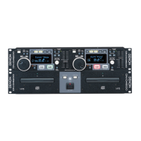
DN-D4500
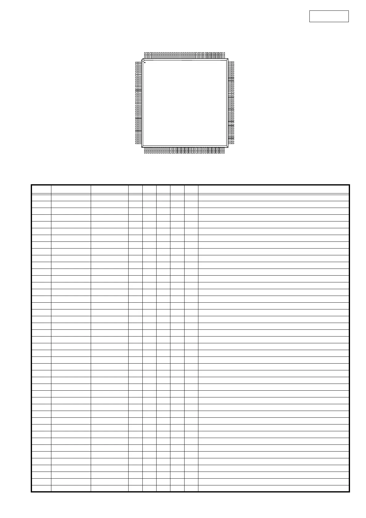
ADSP-BF531 (IC401)
ADSP-BF531 Terminal Function
Pin No. Pin Name Symbol I/O DET Ext Ini Res Function
1GND GND -----GND
2GND GND -----GND
3GND GND -----GND
4VROUT2 O----Ext. FET drive output 2
5VROUT1 VROUT1 O----Ext. FET drive output 1
6VDDEXT VDDEXT I----I/O power supply (+3.3V)
7GND GND -----GND
8GND GND -----GND
9GND GND -----GND
10CLKIN CLKIN I----Clock input
11XTAL XTAL O----Crystal/Oscillation terminal
12VDDEXT VDDEXT I----I/O power supply (+3.3V)
13 _RESET _RESET I ----Reset signal input
14NMI NMI I----Non-maskable interrupt
15GND GND -----GND
16RTXO O----RTC crystal/Oscillation output
17 RTXI I - - L L RTC crystal/Oscillation input
18VDDRTC VDDRTC I----Real Time Clock power supply (+3.3V)
19GND GND -----GND
20VDDEXT VDDEXT I----I/O power supply (+3.3V)
21 PPI_CLK I - - L L PPI clock
22 PPI0 O - - L - PPI data 0
23 PPI1 O - - L - PPI data 1
24 PPI2 O - - L - PPI data 2
25VDDINT VDDINT I----Core power supply (+1.2V)
26 PPI3 O - - L - PPI data 3
27 PF15 O - - L - Programmable flag 15
28 PF14 O - - L - Programmable flag 14
29 PF13 O - - L - Programmable flag 13
30GND GND -----GND
31VDDEXT VDDEXT I----I/O power supply (+3.3V)
32 PF12 O - - L - Programmable flag 12
33 PF11 O - - L - Programmable flag 11
34 PF10 O - - L - Programmable flag 10
35 PF9 O - - L - Programmable flag 9
36 PF8 DEBUG2 O - - L - Debug pin
37 PF7 DEBUG1 O - - L - Debug pin
38 PF6 FSYNC2 O - - L - X2: Clock for playback interrupt input / X1: LRCK (MP3)
39GND GND -----GND
40GND GND -----GND
41GND GND -----GND
42GND GND -----GND
43GND GND -----GND
44GND GND -----GND
PIN 1
133
1
132
45
44
88
89
176
TOP VIEW