EasyManua.ls Logo

Fibocom FM101-GL - 3.6 Status Indicator

Fibocom FM101-GL
78 pages
Print Icon
To Next Page IconTo Next Page
To Previous Page IconTo Previous Page
Loading...
3 Application Interface
Copyright © Fibocom Wireless Inc. 38
3.5.1 USB Interface Definition
Pin
Pin Name
I/O
Reset Value
Pin Description
Level
7
USB D+
I/O
-
USB data plus
0.3-3V
9
USB D-
I/O
-
USB data minus
0.3-3V
29
USB 3.0_TX-
O
-
USB 3.0 transmit data minus
-
31
USB 3.0_TX+
O
-
USB 3.0 transmit data plus
-
35
USB 3.0_RX-
I
-
USB 3.0 receive data minus
-
37
USB 3.0_RX+
I
-
USB 3.0 receive data plus
-
3.5.2 USB2.0 Interface Application
The reference circuit is shown in Figure 14:
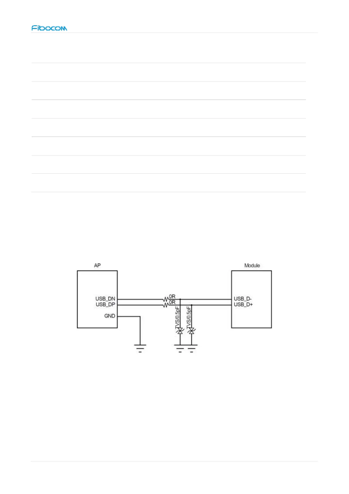
Figure 14 Reference Circuit for USB 2.0 Interface
Since the module supports USB 2.0 High-Speed, it is required to use TVS diodes with
equivalent capacitance of 1pF or smaller ones on the USB_D-/D+ differential signal lines, it
is recommended to use 0.5pF TVS diodes.
USB_D- and USB_D+ are high speed differential signal lines with the maximum transfer rate
of 480 Mbit/s, so the following rules shall be followed carefully in the case of PCB layout:

Related product manuals