EasyManuals Logo

Fibocom L850-GL Series User Manual

Fibocom L850-GL Series
59 pages
To Next Page IconTo Next Page
To Previous Page IconTo Previous Page
Page #22 background imageLoading...
Page #22 background image
Reproduction forbidden without Fibocom Wireless Inc. written authorization - All Rights Reserved.
FIBOCOM L850-GL Series Hardware Guide Page 22 of 59
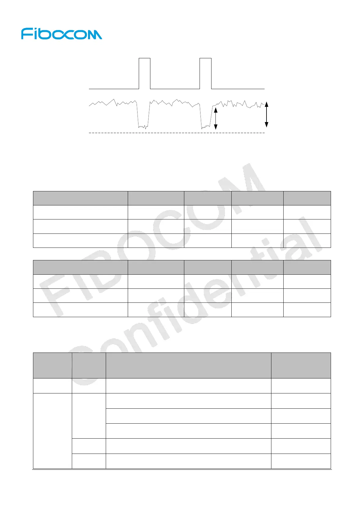
Figure 3-3 Power supply limit
3.2.2 Logic Level
The L850 module 1.8V logic level definition is shown in the following table:
Parameter Minimum Typical Maximum Unit
1.8V logic level 1.71 1.8 1.89 V
V
IH
1.3 1.8 1.89 V
V
IL
-0.3 0 0.3 V
The L850 module 3.3V logic level definition is shown in the following table:
Parameter Minimum Typical Maximum Unit
3.3V logic level 3.135 3.3 3.465 V
V
IH
2.3 3.3 3.465 V
V
IL
-0.3 0 0.3 V
3.2.3 Power Consumption
In the condition of 3.3V power supply, the L850 power consumption is shown in the following table:
Parameter Mode Condition
Average
Current (mA)
I
off
Power off Power supply, module power off 0.05
I
Sleep
WCDMA
DRX=6 3.4
DRX=8 2.8
DRX=9 2.4
LTE FDD Paging cycle #128 frames (1.28s DRx cycle) 3.5
LTE TDD Paging cycle #128 frames (1.28s DRx cycle) 3.8
Burst transmit
Burst transmit
min
:
3
.
135
V
Power supply
Ripple300mV
Drop
VBAT3.135V

Questions and Answers:

Question and Answer IconNeed help?

Do you have a question about the Fibocom L850-GL Series and is the answer not in the manual?

Fibocom L850-GL Series Specifications

General IconGeneral
CategoryGSM/GPRS Modules
ModelL850-GL
Form FactorM.2
Operating Temperature-10°C to +55°C
Storage Temperature-40°C to +85°C
GSM Bands850/900/1800/1900MHz
GNSSGPS, GLONASS, BeiDou, Galileo
InterfaceUSB 2.0, UART, PCM, I2C, GPIO
Operating Voltage3.135V to 4.4V
LTE FDDB1, B2, B3, B4, B5, B7, B8, B12, B13, B17, B18, B19, B20, B25, B26, B28, B29, B30, B66
LTE TDDB38/B39/B40/B41
WCDMAB1, B2, B4, B5, B8
AT Command Set3GPP TS 27.007
CertificationsCE, FCC, GCF, PTCRB