Reproduction forbidden without Fibocom Wireless Inc. written authorization - All Rights Reserved.
FIBOCOM L850-GL Series Hardware Guide Page 30 of 59
PCIe Link State PERST# CLKREQ#
Power Consumption
Description
D0 L1.2 H H I
sleep
Refer 3.2.3 Power Consumption
D3
cold
L2
L H I
sleep
+0.5
The extra 0.5mA is consumed on
PERST# pull down
L L I
sleep
+0.8
The extra 0.3mA is consumed on
CLKREQ# pull down
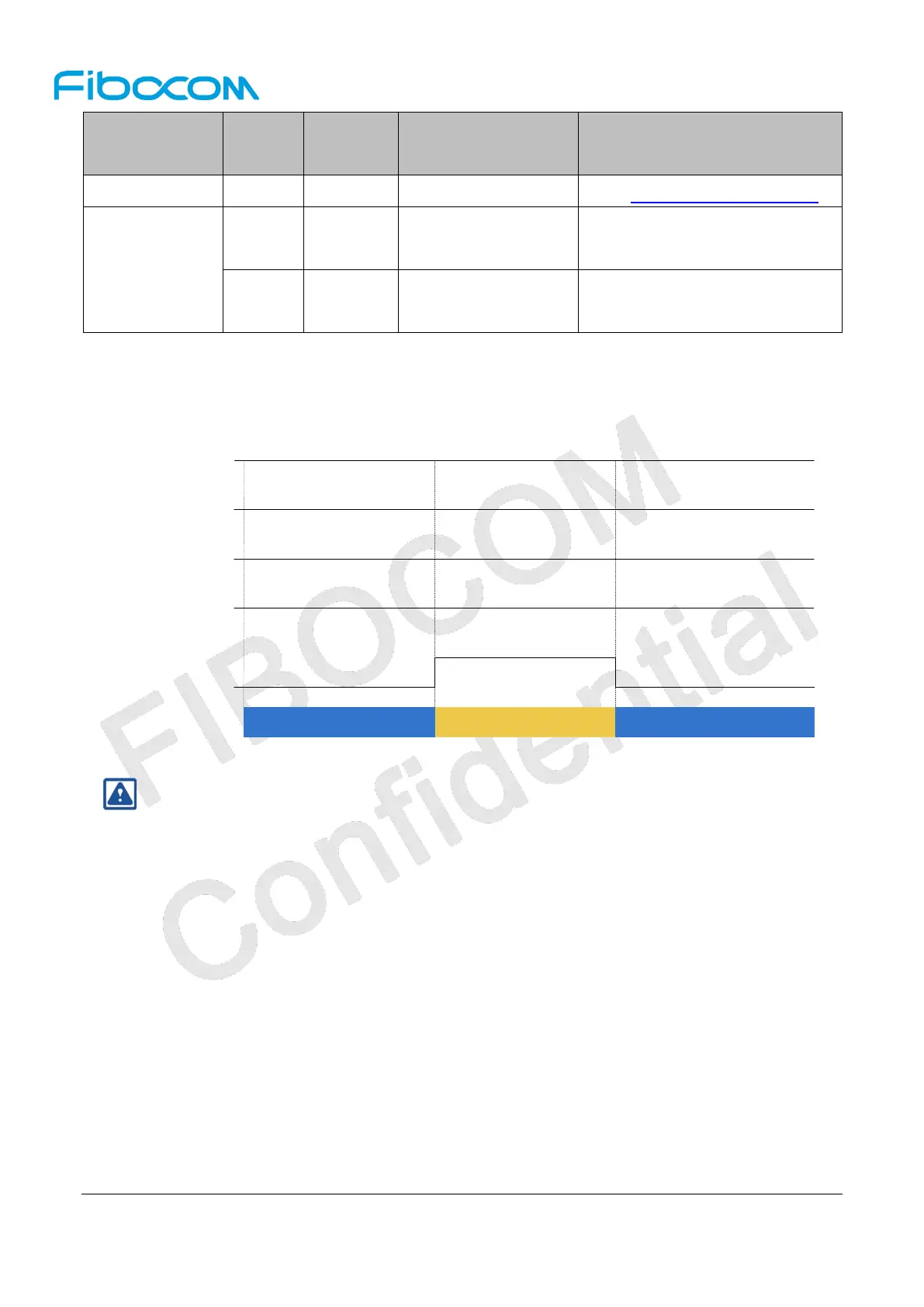
3.3.4.1 D0 L1.2
Module supports PCIe goes into D0 L1.2 state in Win10 system. The D0 L0@S0/S0ix→
D0 L1.2@S0/S0ix→D0 L0@S0/S0ix timing is shown in figure 3-10:
+3.3V
PERST#
RESET#
Module State
D0 L1.2@S0/S0ixD0 L0@S0/S0ix
FCPO#
D0 L0@S0/S0ix
CLKREQ
#
Figure 3-10 D0 L1.2 timi
Note
:
When USB is used as data transfer interface in Chrome/Android/Linux OS, there is no PCIe link
state. But when USB goes into suspend it also needs to follow the timing above (If PERST# and
CLKREQ# are floating, don’t control PERST# and CLKREQ#).
3.3.4.2 D3
cold
L2
Module supports PCIe goes into D3
cold
L2 state in Win10 system. In D3
cold
L2 state, PCIe link can be
woken up by both modem and host. The D0 L0@S0/S0ix→D3
cold
L2@S0/S0ix→D0 L0@S0/S0ix timing
is shown in Figure 3-11 and Figure 3-12:
 Loading...