Reproduction forbidden without Fibocom Wireless Inc. written authorization - All Rights Reserved.
FIBOCOM L850-GL Series Hardware Guide Page 36 of 59
configured in practical application.
3.4.2.1 USB Interface Definition
Pin# Pin Name I/O Description Type
7 USB_D+ I/O USB data plus
0.3---3V,
USB2.0
9 USB_D- I/O USB data minus
0.3---3V,
USB2.0
29 USB3.0_TX- O USB3.0 transmit data minus -
31 USB3.0_TX+ O USB3.0 transmit data plus -
35 USB3.0_RX- I USB3.0 receive data minus -
37 USB3.0_RX+ I USB3.0 receive data plus -
3.4.2.2 USB2.0 Interface Application
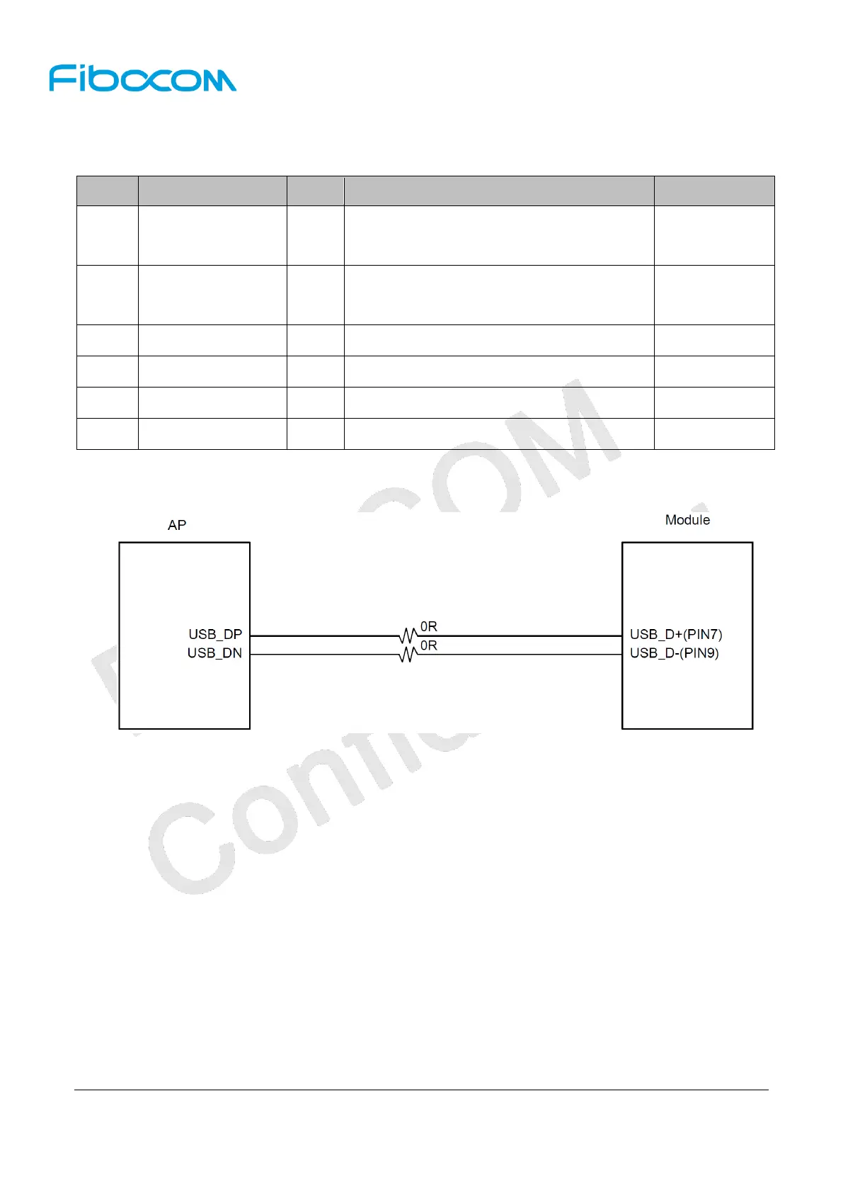
The reference circuit is shown in Figure 3-16:
Figure 3-16 Reference circuit for USB 2.0 interface
USB_D- and USB_D+ are high speed differential signal lines with the maximum transfer rate of 480 Mbps,
so the following rules should be followed carefully in the case of PCB layout:
USB_D- and USB_D+ signal lines should have the differential impedance of 90Ω.
USB_D- and USB_D+ signal lines should be parallel and have the equal length. The right angle routing
should be avoided.
USB_D- and USB_D+ signal lines should be routed on the layer that is adjacent to the ground layer,
and wrapped with GND vertically and horizontally.
3.4.2.3 USB3.0 Interface Application
The reference circuit is shown in Figure 3-17:
 Loading...