Reproduction forbidden without Fibocom Wireless Inc. written authorization - All Rights Reserved.
FIBOCOM L850-GL Series Hardware Guide Page 37 of 59
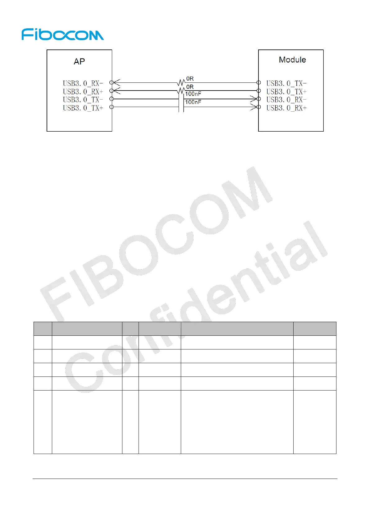
Figure 3-17 Reference circuit for USB3.0 interface
USB3.0 signals are super speed differential signal lines with the maximum transfer rate of 5 Gbps. So the
following rules should be followed carefully in the case of PCB layout:
USB3.0_TX-/USB3.0_TX+ and USB3.0_RX-/ USB3.0_RX+ are two pairs differential signal lines. The
differential impedance should be controlled as 90Ω.
The two pairs differential signal lines should be parallel and have the equal length. The right angle
routing should be avoided.
The two pairs differential signal lines should be routed on the layer that is adjacent to the ground layer,
and wrapped with GND vertically and horizontally.
3.5 USIM Interface
The L850 module has a built-in USIM card interface, which supports 1.8V and 3V SIM cards.
3.5.1 USIM Pins
The USIM pins description is shown in the following table:
Pin Pin Name I/O Reset Value Description Type
36 UIM_PWR PO
-
USIM power supply 1.8V/3V
30 UIM_RESET O L USIM reset 1.8V/3V
32 UIM_CLK O L USIM clock 1.8V/3V
34 UIM_DATA I/O L USIM data, internal pull up(4.7KΩ) 1.8V/3V
66 SIM_DETECT I PD
USIM card detect, internal 390K pull-
up.
Active high, and high level indicates
SIM card is inserted; and low level
indicates SIM card is detached.
1.8V
 Loading...