Reproduction forbidden without Fibocom Wireless Inc. written authorization - All Rights Reserved.
FIBOCOM L850-GL Series Hardware Guide Page 25 of 59
3.3 Control Signal
The L850 module provides two control signals for power on/off and reset operations. The pin is defined in
the following table:
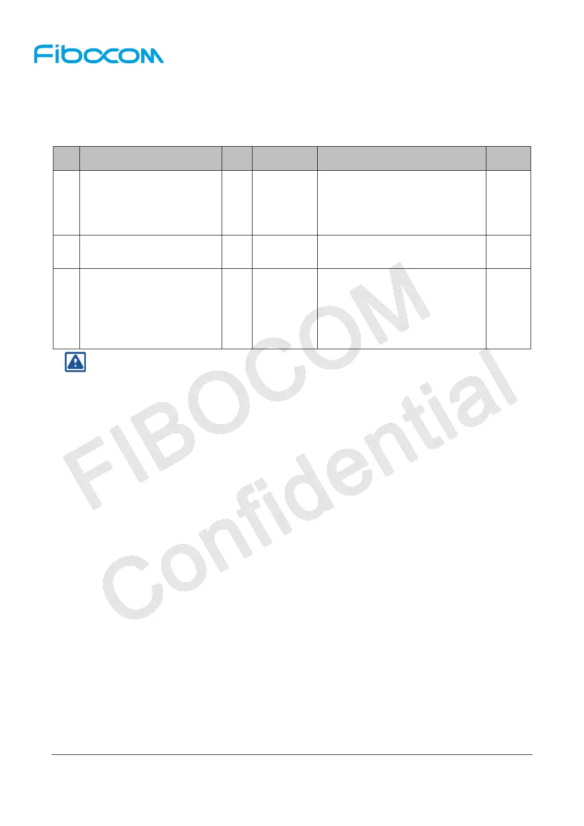
Pin Pin Name I/O Reset Value Functions Type
6 FULL_CARD_POWER_OFF#
I
PU
Module power on/off input,
internal pull up
Power on: High/Floating
Power off: Low
3.3/1.8V
67 RESET# I
-
WWAN reset input, internal pull
up(10KΩ), active low
1.8V
50 PERST# I PU
Asserted to reset module PCIe
interface default. If module went
into core dump, it will reset whole
module, not only PCIe interface.
Active low, internal pull up(10KΩ)
3.3V
Note:
RESET# and PERST# need to be controlled by independent GPIO, and not shared with other
devices on the host. RESET# and PERST# are sensitive signals, so they should keep away from
RF interference and be protected by GND. It should be neither near PCB edge nor route on
surface layer to avoid module abnormal reset caused by ESD.
3.3.1 Module Start-Up
3.3.1.1 Start-up Circuit
The FCPO# (FULL_CARD_POWER_OFF#) pin needs an external 3.3V or 1.8V pull up for booting up. AP
(Application Processor) controls module start-up. The recommended design is using a default PD port to
control FCPO#. It also should reserve a 100K pull down resistor on AP side. The reference design is shown
in Figure3-4:
 Loading...