vii
List of Figures
Figure Title Page
1-1. Volt-Hertz Capability............................................................................................1-15
2-1. Line Power Cords Available for Fluke Instruments..............................................2-4
2-2. Correct Way to Dress Interface Cable...................................................................2-6
2-3. Line Power Label and Switch Location.................................................................2-7
2-4. Accessing the Fuse................................................................................................2-8
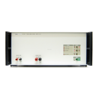
3-1. Front Panel Features..............................................................................................3-4
3-2. Rear Panel Features...............................................................................................3-6
3-3. Standby Mode Indicator.........................................................................................3-9
3-4. Voltage Standby Mode..........................................................................................3-10
3-5. Current Standby Mode...........................................................................................3-11
3-6. Voltage Operate Mode...........................................................................................3-12
3-7. Current Operate Mode...........................................................................................3-13
4-1. 5725A Overall Block Diagram..............................................................................4-4
4-2. Digital Assembly Block Diagram..........................................................................4-17
4-3. Current Amplifier Assembly Block Diagram........................................................4-20
4-4. High Voltage Amplifier Assembly Block Diagram..............................................4-25
4-5. High Voltage Sense Assembly Block Diagram.....................................................4-31
6-1. Accessing the Fuse................................................................................................6-4
6-2. Accessing the Air Filter.........................................................................................6-5
6-3. Assembly Location Diagram.................................................................................6-6
6-4. Initial Access Procedure........................................................................................6-8
6-5. Accessing the Digital Assembly............................................................................6-10
6-6. Correct Way to Dress Cables.................................................................................6-12
6-7. Enabling Front or Rear Binding Posts...................................................................6-16
8-1. Final Assembly......................................................................................................8-7
8-2. A1 Interconnect PCA.............................................................................................8-16
8-3. A2 Current Amplifier PCA....................................................................................8-20
8-4. A3 High Voltage Amplifier PCA..........................................................................8-24
8-5. A4 Power Supply PCA..........................................................................................8-28
8-6. A5 Digital PCA......................................................................................................8-30
8-7. A6 High Voltage Sense PCA.................................................................................8-34
8-8. A12 Transformer Enclosure Assembly..................................................................8-36