v
Illustrations
Figures
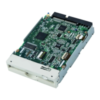
Figure 1.1 Outer view (with panel) 1-6
Figure 1.2 Outer view (without panel) 1-6
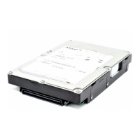
Figure 1.3 Optical disk drive configuration 1-7
Figure 1.4 Control circuit section block diagram 1-8
Figure 1.5 System configuration with one optical disk drive 1-10
Figure 1.6 System configuration with two optical disk drives 1–10
Figure 2.1 Optical disk cartridge 2-8
Figure 2.2 Algorithms for alternate processing 2-11
Figure 2.3 Example of alternate processing 2–12
Figure 3.1 Surface temperature measurement points 3-2
Figure 3.2 Dimensions 3-6
Figure 3.3 Dimensions (without panel) 3-7
Figure 3.4 Installation directions 3-8
Figure 3.5 Centers of gravity 3-9
Figure 3.6 Mounting frame structure 3-10
Figure 3.7 Service clearance 3-11
Figure 3.8 Current waveform (+5 VDC) 3-12
Figure 3.9 Connector and terminal locations 3-13
Figure 3.10 Cable connection diagram 3-14
Figure 3.11 Jumper settings at factory shipping 3-15
Figure 3.12 Master device setting 3-15
Figure 3.13 Slave device setting 3-16
Figure 3.14 Cable select mode setting 3-16
Figure 3.15 Cable select examples 3-17
Figure 3.16 Individual packaging style 3-20
Figure 4.1 Power mode 4-19
Figure 4.2 Register/PIO data transfer 4-78
Figure 4.3 Multiword DMA data transfer 4-80
Figure 4.4 Ultra DMA data in transfer (initialization timing) 4-82
Figure 4.5 Ultra DMA data in transfer (continuous transfer timing) 4-82
Figure 4.6 Ultra DMA data in transfer (host stop timing) 4-83
Figure 4.7 Ultra DMA data in transfer (device end timing) 4-83
Figure 4.8 Ultra DMA data in transfer (host end timing) 4-84
Figure 4.9 Ultra DMA data out transfer (initialization timing) 4-85