U5
RF GAIN VR
AGC OFF
S
RT4
U4 1/2
U4 2/2
AGC FAST
U3 2/2
U3 1/2
R60
C77
R61
U21
R62 Q21
U1, 2
Q39
CPU
Figure 2-18 AGC and Demodulator Circuits
In the AM demodulating circuit, the receiving signal (455 kHz) is amplified by Q19, de-
tected by CR21/22, and derives audio signal.
In the SSB demodulating circuit (including TLX), the receiving signal (455 kHz) is am-
plified by Q20, mixed with 3Lo (456.5 kHz) by CR22 (demodulation), and derives audio
signal.
Note)
The CPU reads RF gain voltage, converts from analog signal to digital signal,
and processes the signal for an adequate curve to control the AGC circuit. RF gain can
be changed by MIF command RF xx output from an external unit. Rotating RF GAIN
volume cancels the MIF command.
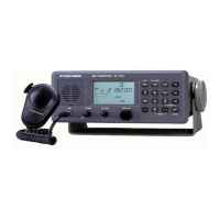
TX/RX Section AF
The received AF signal is distributed through each analog switch to LINE OUT, SQ SIG
(for audio squelch signal detection), SPEAKER output, and PHONE output circuit.
SQ SIG detecting circuit U10 outputs "SQ SIG" to CPU. CPU analyses the frequency
components of this signal, outputs RX AF OFF signal through U12, and controls U20-5
and -13 lines for squelch control. While intercom is used and self-testing, the RX AF
OFF signal switches the U20 lines (RX line) OFF.
MUTE signal from CPU directly switches OFF U20-5 and 13 lines when transmitting
from MIC, and remote terminal, tow-tone alarming, tuning antenna coupler, using inter-
com, and self-testing.
 Loading...