2-26
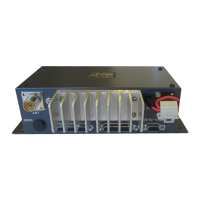
2.6 Power Supply SW Circuit
Power supply SW circuit is included in PA/FIL board.
When the power switch is turned on, a relay K1 is made ON by Q1 and power is supplied
to circuits. To protect the contact of K1 against the rush current at power on, a delay cir-
cuit is provided. That is, C10 is charged through Q11 which is switched on by Q3 at
power on, and then K1 is turned on. When K1 is ON, Q11 is switched OFF, and power is
supplied through K1. Turn-on of K1 is delayed until C9 is charged.
K1
Overvolt.
Detector
+12 V
-12 V
+ 13.6 V
– 13.6 V
FL2
F2 (1.35 A)
CR1 Q11
R2
K1
F1 (4 A)
C10
R1
R4
Q3
Q2
Q1
C13 C14
C49 to 52
PA
EE
U1
POWER SW
BK + 12V
BK – 12V
JP1
JP2
TB1
TB2
TX/RX PCB
SW REG
(OPTION)
J1
J3 J4
J2
12 V
J7
12 V
J1
POWER ON
+13.6 V
R12
C9
Figure 2-20 Power Supply Circuit
The allowable input voltage of power supply is from about +8 V to +17 V. (Rating volt-
age: 13.6 V
±
15 %) The upper limit +17V is determined by a over-voltage detector U1
and a switch Q2 and the lower limit +8 V is determined by the drive voltage of the relay
K1. F1 and F2 are poly-switches. The poly-switch works as a fuse that cuts off (trip) cir-
cuit with a Joule heat generated by the current flowing through it. Once the switch be-
comes off, it does not recover until it cools down while power supply is off.
Note)
The negative line of the power supply and the negative ground of the circuit
boards (chassis) shares a common earth. When a floating ground that separates the
negative line and the negative ground is needed, an optional SW REG board is to be
added.
 Loading...