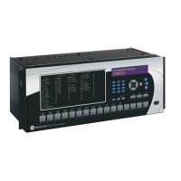
GE Multilin N60 Network Stability and Synchrophasor Measurement System B-45
APPENDIX B B.4 MEMORY MAPPING
B
81AE Direct Analog Input 24 Value 0 to 2147483647 --- 0.01 F060 0
81B0 Direct Analog Input 25 Value 0 to 2147483647 --- 0.01 F060 0
81B2 Direct Analog Input 26 Value 0 to 2147483647 --- 0.01 F060 0
81B4 Direct Analog Input 27 Value 0 to 2147483647 --- 0.01 F060 0
81B6 Direct Analog Input 28 Value 0 to 2147483647 --- 0.01 F060 0
81B8 Direct Analog Input 29 Value 0 to 2147483647 --- 0.01 F060 0
81BA Direct Analog Input 30 Value 0 to 2147483647 --- 0.01 F060 0
81BC Direct Analog Input 31 Value 0 to 2147483647 --- 0.01 F060 0
81BE Direct Analog Input 32 Value 0 to 2147483647 --- 0.01 F060 0
Temp Monitor Actual Values (Read Only Non-Volatile)
81C0 Reserved Register T1 -55 to 125 C 1 F002 -55
81C1 Reserved Register T2 -55 to 125 C 1 F002 125
81C2 Reserved Register T3 -2147483647 to
2147483647
--- 1 F004 0
81C4 Reserved Register T4 0 to 4294967295 --- 1 F003 0
81C6 Reserved Register T5 0 to 4294967295 --- 1 F003 0
81C8 Reserved Register T6 0 to 4294967295 --- 1 F003 0
81CA Reserved Register T7 0 to 4294967295 --- 1 F003 0
81CC Reserved Register T8 0 to 4294967295 --- 1 F003 0
Summator Actual Values (Read Only)
81D0 Summator 1 Actual Value –9999999999 to
9999999999
--- 1 F060 0
81D2 Summator 2 Actual Value –9999999999 to
9999999999
--- 1 F060 0
81D4 Summator 3 Actual Value –9999999999 to
9999999999
--- 1 F060 0
81D6 Summator 4 Actual Value –9999999999 to
9999999999
1F060 0
81D8 Summator 5 Actual Value –9999999999 to
9999999999
1F060 0
81DA Summator 6 Actual Value –9999999999 to
9999999999
1F060 0
Digitizer Settings (Read/Write) (5 Modules)
8260 Digitizer 1 Function 0 to 1 --- 1 F102 0 (Disabled)
8261 Digitizer 1 Source Input 0 to 65535 --- 1 F600 0
8262 Digitizer 1 Limit Setting 0.05 to 90 pu 0.001 F003 1000
8264 Reserved (4 items) 0 to 65535 --- 1 F001 0
8268 ...Repeated for digitizer 2
8270 ...Repeated for digitizer 3
8278 ...Repeated for digitizer 4
8280 ...Repeated for digitizer 5
Digitizer Actual Values (Read Only) (5 Modules)
82A0 Digitizer 1 Output -127 to 127 --- 1 F004 0
82A2 Digitizer 2 Output -127 to 127 --- 1 F004 0
82A4 Digitizer 3 Output -127 to 127 --- 1 F004 0
82A6 Digitizer 4 Output -127 to 127 --- 1 F004 0
82A8 Digitizer 5 Output -127 to 127 --- 1 F004 0
Switch (Read/Write Setting) (6 Modules)
82C0 Switch 1 Function 0 to 1 --- 1 F102 0 (Disabled)
82C1 Switch 1 Argument A Bits (8 items) 0 to 4294967295 --- 1 F300 0
82D9 Switch 1 Argument B Bits (8 items) 0 to 4294967295 --- 1 F300 0
82E1 Switch 1 Control 0 to 4294967295 --- 1 F300 0
82E3 Reserved (6 items) 0 to 4294967295 --- 1 F001 0
82E9 ...Repeated for Switch 2
8312 ...Repeated for Switch 3
833B ...Repeated for Switch 4
Table B–10: MODBUS MEMORY MAP (Sheet 37 of 70)
ADDR REGISTER NAME RANGE UNITS STEP FORMAT DEFAULT