Page
1 00
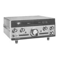
Heathkit
during transmit. At this time, emitter followers
Q114
and
Q115
are also turned on
by
the "+T" switching
voltage. The
8.8307
MHz output signal at the emitter
(E) of
Q115
is coupled through
C217, where its
amplitude
is controlled by CW Level control
R2.
This controlled level is coupled through
C218
to a
low-pass filter to suppress the harmonic
output of
the BFO. The filtered BFO signal
is coupled
to
2nd
mixer U401.
2ND MIXER
U401 is a double-balanced mixer that is
used in both
the receive and transmit modes of operation.
In
transmit, D303
is forward
biased and the TX sig-
nal is fed from the BFO
to U401,
where
the signal
is mixed
with
the premix signal supplied
by
Q101
on the oscillator circuit board. At the same time,
a +12 volt switching voltage
(
+
R) is removed from
the anode end of D301 and
D302, and
"
+
T" applies
a reverse bias voltage
to these diodes.
The signal
at
the
output (pin
1)
of U401 is coupled
through impedance-matching transformer
T401 to
the
input of the selected
bandpass filter (one of
eight
possible filters). A "+T" voltage
is applied to the
anode
of D401, which permits the signal
to be
coupled to the
base
of
Q401. At the same time, the
"
+
T"
voltage
is also applied to the cathode
of D403,
which isolates
the
receive
line from the
transmit
line.
From the emitter of amplifier
Q401,
the signal is fed
to the base of amplifier
Q402;
and
from Q402's emit-
ter,
the signal is
applied
to the base of driver
Q404.
At this time, keying transistor
Q403
keeps
Q404
turned on.
Q404
amplifies the signal,
couples it
through impedance-matching transformer T402, and
then applies the signal
to
the
base
of
each of the
two PA transistors,
Q405
and
Q406.
Zener
diode
D405 prevents excessive
RF
voltages
on the collec-
tors of these transistors from
destroying them under
no-load and high-SWR conditions.
From
the output of the PA transistors, the amplified
RF signal is fed to
matching transformer T403
and
then coupled to the low-pass filter in use for that
band. The resulting filtered signal is then applied
to antenna jack
J4.
In receive,
the signals
received
by the
antenna
are
coupled through
the proper
low-pass
filter
and
C443. A "+R" voltage
is
applied to
the anode
of
D404
and D407,
which
allow the
signal to
pass
through
matching
transformer
T404 and
continue
through
the selected
bandpass
filter; thus
taking
the
same path
(but opposite
direction)
as the
transmit
signal
to the 2nd mixer.
At
the 2nd mixer,
the receive
signal is
mixed
with
the premix
signal; thus,
a resulting
8.83 MHz
IF sig-
nal
is coupled through
switching
diodes
D302
and
D301, which
are forward
biased
by the
"
+
R" volt-
age. This
signal
is now coupled
through
matching
transformer
T301
to the gate
of common
source IF
amplifier
Q301,
which
receives
its
operating voltage
from
the switched
"
+ R" line.
The resulting
IF signal
passes through
FL301
and is further
amplified
by
2nd
IF amplifier
U301. From
the
output of
U301,
the
amplified signal
is coupled
to matching
trans-
former
T302.
C327 couples
a
portion
of the
signal
at the output
of T302
to the AGC loop.
This signal
is now
rectified
by D309
and D311
and filtered
by
C328.
The
result-
ing negative
voltage is
fed to the input
(pin
2)
of
AGC
amplifier
U302. A fixed
positive
reference volt-
age is applied
to pin
3 of U302.
When the
strength
of
the signal
that the transceiver
is
tuned to
in-
creases, the voltage
at
pin
2 of U302
decreases
(goes
more
negative).
This produces
a higher
positive volt-
age at the
output (pin
6)
of
U302. As this voltage
increases,
D305 starts
to conduct.
This allows
C317
to charge, resulting
in
a positive voltage
being
ap-
plied
to pin
5
of 2nd
IF amplifier
U301;
thus, the
gain of U301 is
reduced. R312
provides
a discharge
path for
C317.
The
amplified
8.83 MHz IF signal
is coupled
through
C326 to the
signal input
(pin
4)
of
product
detector
U303.
A signal from
the BFO
is coupled
through
C329 to the carrier input
(pin
7)
of
U303.
U303 mixes
the two input
signals and
produces
sum and
differ-
ence
signals
at
its
output (pin
6).
The sum
frequency
is filtered
out by
C334 through
C336. The difference
frequency
is an audio
signal.