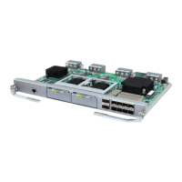
Figure 5-14 SLPU..............................................................................................................................................5-19
Figure 5-15 Slots of the SLPU...........................................................................................................................5-19
Figure 5-16 UELP panel.....................................................................................................................................5-20
Figure 5-17 DIP switch on the UELP................................................................................................................5-21
Figure 5-18 Panel of the UFLP..........................................................................................................................5-22
Figure 5-19 Panel of the USLP2........................................................................................................................5-23
Figure 5-20 Mapping relationship between the pins in the input and output ports on the USLP2....................5-23
BBU3900
Hardware Description Figures
Issue 11 (2010-11-10) Huawei Proprietary and Confidential
Copyright © Huawei Technologies Co., Ltd.
xi
 Loading...