42 IBM Power 770 and 780 (9117-MMD, 9179-MHD) Technical Overview and Introduction
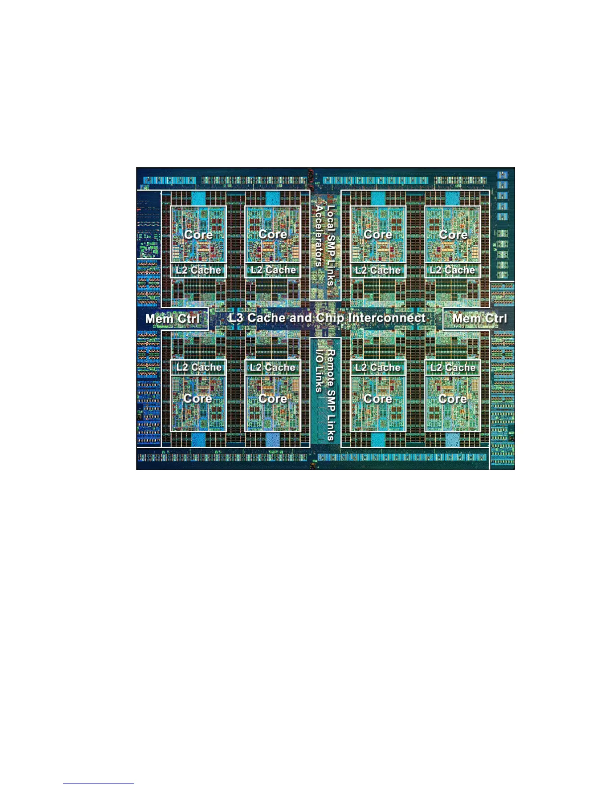
Figure 2-2 shows the POWER7+ processor die layout, with the major areas identified:
Processor cores
L2 cache
L3 cache and chip interconnection
Simultaneous multiprocessing links
Memory controllers.
I/O links
Figure 2-2 POWER7+ processor die with key areas indicated
2.1.1 POWER7+ processor overview
The POWER7+ processor chip is fabricated with IBM 32 nm Silicon-On-Insulator (SOI)
technology using copper interconnect, and implements an on-chip L3 cache using eDRAM.
The POWER7+ processor chip is 567 mm
2
and is built by using 2.1 billion components
(transistors). Up to eight processor cores are on the chip, each with 12 execution units,
256 KB of L2 cache per core, and access to up to 80 MB of shared on-chip L3 cache per
SCM.
For memory access, the POWER7+ processor includes one double data rate 3 (DDR3)
memory controllers, each with four memory channels. To be able to scale effectively, the
POWER7+ processor uses a combination of local and global SMP links with high coherency
bandwidth and takes advantage of the IBM dual-scope broadcast coherence protocol.